
Page 48 - Power Electronics Handbook
P. 48
Thyristors 41
r PC
PC
R2
(d) be
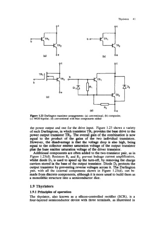
Figure 1.23 Darlington transistor arrangements: (a) conventional; (b) composite;
(c) MOS-bipolar; (d) conventional with bias components added
the power output and one for the drive input. Figure 1.23 shows a variety
of such Darlingtons, in which transistor TRl provides the base drive to the
power output transistor TR2. The overall gain of the combination is now
equal to the product of the gains of the two individual transistors.
However, the disadvantage is that the voltage drop is also high, being
equal to the collector emitter saturation voltage of the output transistor
plus the base emitter saturation voltage of the driver transistor.
Additional components are often added to the two-transistor pair, as in
Figure 1.23(d). Resistors R, and R2 prevent leakage current amplification,
whilst diode D1 is used to speed up the turn-off, by removing the charge
carriers stored in the base of the output transistor. Diode Dz protects the
output transistor by preventing reverse voltages across it. The Darlington
pair, with all the external components shown in Figure 1.23(d), can be
made from discrete components, although it is more usual to build them as
a monolithic structure into a semiconductor dice.
1.9 Thyristors
1.9.1 Prindples of operation
The thyristor, also known as a silicon-controlled rectifier (SCR), is a
four-layered semiconductor device with three terminals, as illustrated in