
Page 53 - Power Electronics Handbook
P. 53
46 Power semiconductor devices
The switching characteristic of a thyristor determines its switching losses
and maximum operating frequency, much as it did for the transistor. The
shape of the turn-on curve is very similar to Figure 1.12, where the current
through the device rises as the anode-to-cathode voltage falls. The time for
10% turn-on, measured from the application of gate drive, is called the
delay time, and that between 10% and 90% is the rise time. The sum of the
delay and rise times is the turn-on time of the thyristor. The turn-on time is
reduced if a steep rising gate pulse is used and the power in this drive is
increased.
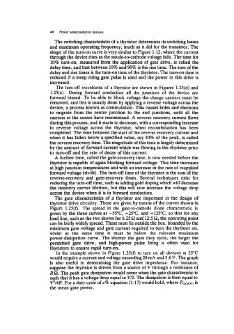
The turn-off waveforms of a thyristor are shown in Figures 1.25(d) and
1.25(e). During forward conduction all the junctions of the device are
forward biased. To be able to block voltage the charge carriers must be
removed, and this is usually done by applying a reverse voltage across the
device, a process known as commutation. This causes holes and electrons
to migrate from the centre junction to the end junctions, until all the
carriers at the centre have recombined. A reverse recovery current flows
during this process, and it starts to decrease, with a corresponding increase
in reverse voltage across the thyristor, when recombination has been
completed. The time between the start of the reverse recovery current and
when it has fallen below a specified value, say 20% of the peak, is called
the reverse recovery time. The magnitude of this time is largely determined
by the amount of forward current which was flowing in the thyristor prior
to turn-off and the rate of decay of this current.
A further time, called the gate-recovery time, is now needed before the
thyristor is capable of again blocking forward voltage. This time increases
at high junction temperatures and with an increase in the rate of reapplied
forward voltage (dv/dt). The turn-off time of the thyristor is the sum of the
reverse-recovery and gate-recovery times. Several techniques exist for
reducing the turn-off time, such as adding gold doping which will decrease
the minority carrier lifetime, but this will now increase the voltage drop
across the device when it is in forward conduction.
The gate characteristics of a thyristor are important in the design of
thyristor drive circuitry. These are given by means of the curves shown in
Figure 1.25(f). The spread in the gate-to-cathode diode characteristic is
given by the three curves at -55"C, +25"C, and +125"C, so that for any
load line, such as the two shown for 6.25 P and 12.5 52, the operating point
can be fairly widely spread. These must lie outside the box, bounded by the
minimum gate voltage and gate current required to turn the thyristor on,
whilst at the same time it must be below the relevant maximum
power-dissipation curve. The shorter the gate duty cycle, the larger the
permitted gate drive, and high-power pulse firing is often used for
thyristors to ensure rapid turn-on.
In the example shown in Figure 1.25(f) to turn on all devices at 25°C
would require a current and voltage exceeding 20 mA and 3.0 V. The graph
is also useful in determining the gate drive impedance. For instance,
suppose the thyristor is driven from a source of V through a resistance of
R 9. The peak gate dissipation would occur when the gate characteristic is
such that it has a voltage drop equal to V/2. The dissipation is then equal to
p4R. For a duty cycle of x% equation (1.17) would hold, where PG(AV) is
the mean gate power.