
Page 60 - Power Electronics Handbook
P. 60
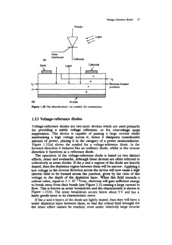
Voltage-reference. diodes   53


                                            I Anode


                                Gate
                                (optional)
                          (a)               I Cathode
                                                     Cathode


                                                                      rse biased
                                                                      ion


                    (b)                   Anobe
                    Figure 1.30 The photothyristor: (a)  symbol; (b) construction


                    1.13 Voltage-reference diodes

                    Voltage-reference diodes are two-layer devices which are used primarily
                    for  providing  a  stable  voltage  reference,  or  for  overvoltage  surge
                    suppression.  The  device  is  capable  of  passing  a  large  current  whilst
                    maintaining a  high  voltage  across  it,  hence  it  dissipates  considerable
                    amount of  power, placing it in the category of  a power semiconductor.
                    Figure  1.31(a) shows the  symbol  for  a  voltage-reference diode.  In  the
                    forward direction it behaves like an ordinary diode, whilst in the reverse
                    direction it functions as a reference diode.
                      The operation of  the voltage-reference diode is based on two distinct
                    effects, zener and avalanche, although these devices are often referred to
                    collectively as zener diodes. If the p and n regions of  the diode are heavily
                    doped, then the depletion region between them will be narrow. Applying a
                    low voltage in the reverse direction across the device will now caw  a high
                    electric field to be formed across the junction, given by  the ratio of this
                    voltage to the  depth of  the  depktion layer.  When this field exceeds a
                    critid value, equal to 3 x 10-~ ~cm, electrons will gain sufficient energy
                    to break away from their bonds (see figure 1.5) causing a large cumnt to
                    flow. This is known as zener breakdown and the characteristic is shown in
                    Figure  1.31@). The zener breakdown  occurs below about  5 V and has  a
                    fairly gentle knee in its characteristic curve.
                      If the p and n layers of the diode are lightly doped, then they will have a
                    wider depletion layer between them, so  that the critical field strength for
                    the zener effect cannot be reached, even under relatively large reverse