
Page 164 - Principles and Applications of NanoMEMS Physics
P. 164
152 Chapter 4
(a)
I I I I
SL SL
SL
SL
(1) I
(1) I (V) (2) I SL
SL (V)
(2) I (t) (t)
SL
SL
t t
1 2 3 4 5 6 7 8 9 10 11
1 2 3 4 5 6 7 8 9 10 11
V V 1 2 3 4 4 3 2 1
1 2 3 4 4 3 2 1
SL
SL
dI /dt (3)
SL /dt
dI
(3)
SL
(4) V (t) (t)
(4) V SL t t
SL
1 2 3 4 4 3 2 1
1 2 3 4 4 3 2 1
1 2 3 4 4 3 2 1
1 2 3 4 4 3 2 1
t t
(b)
Differentiating Differentiating Device Device Integrating Integrating Device Device
Input
Input
V V in in Device N-bit Digital
Device
Digital
N-bit
Output
Latch
Code
Code
Dτ Counting Counting Device Device Latch . . . . . . Output
Dτ
Switching
Switching
Device
Device
+ +
- -
(c)
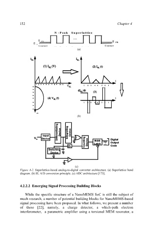
Figure 4-2. Superlattice-based analog-to-digital converter architecture. (a) Superlattice band
diagram. (b) SL A/D conversion principle. (c) ADC architecture [175].
4.2.2.2 Emerging Signal Processing Building Blocks
While the specific structure of a NanoMEMS SoC is still the subject of
much research, a number of potential building blocks for NanoMEMS-based
signal processing have been proposed. In what follows, we present a number
of these [22], namely, a charge detector, a which-path electron
interferometer, a parametric amplifier using a torsional MEM resonator, a