
Page 198 - Principles and Applications of NanoMEMS Physics
P. 198
186 Chapter 4
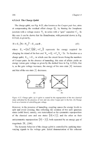
4.3.1.4.1 The Charge Qubit
The charge qubit, see Fig. 4-22, also known as the Cooper pair box, aims
at compensating the residual offset charge Q by biasing the Josephson
r
junction with a voltage source V in series with a “gate” capacitor C . In
g g
this case it can be shown that the Hamiltonian, with potential shown in Fig.
4-21(d), is given by,
2
H = E ( − NN ) − E cos θ , (4 )
3
C g J
where E = () (2e2 2 (C + C )) represents the energy required for
C J g
charging the island of the box and N = Q + C V e 2 / . To function as a
g r g g
charge qubit, E > E , in which case the circuit favors fixing the numbers
CJ J
of Cooper pairs. In the absence of tunneling, this state of affairs yields an
energy versus gate voltage as given by the dashed lines in Fig. 4-22(b), that
is, as the gate voltage increases, the energy of the zero state 0 increases
and that of the one state 1 decreases.
C C C
g g g
E/E C E/E C E/E C
V V V 2E
2E
2E
g g g J J J
Cooper-
Cooper-
Cooper-
Pair Box
Pair Box
Pair Box
0.5
0.5
0.5
2e 2e
C C g VC g V gg V g g 2e
(a) (b)
Figure 4- 2. Charge qubit. (a) A qubit is created by the superposition of the two classical
2
states embodied by the presence of zero and one extra Cooper pair in the box. (b) Energy
levels as a function of controlling gate voltage.
However, in the presence of tunneling, coupling causes the energy levels to
split and avoid crossing, thus reflecting the creation of two new quantum
states (solid lines), namely, one materialized as the symmetric superposition
of the classical zero and one states ( 0 + 1 ), and the other as their
antisymmetric superposition ( 0 − 1 ), both separated by an energy gap of
magnitude E2 [208].
J
The dynamic behavior of the charge qubit is controlled by applying time-
varying signals to the voltage gate. Initial demonstration of the coherent