
Page 318 - Programming Microcontrollers in C
P. 318
A Pulse Width Modulation Program 303
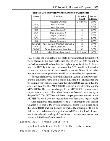
Table 6-2: GPT Interrupt Priorities And Vector Addresses
Name Function Priority Vector
Level Address
Adjusted Channel 0 (highest) 0xV0
IC1 Input Capture 1 1 0xV1
IC2 Input Capture 1 2 0xV2
IC3 Input Capture 3 3 0xV3
OC1 Output Capture 1 4 0xV4
OC2 Output Capture 2 5 0xV5
OC3 Output Capture 3 6 0xV6
IC4 Output Capture 4 7 0xV7
IC4/OC5 Input Capture 4/Output Capture 5 8 0xV8
TCF Timer Overflow 9 0xV9
PAOVF Pulse Accumulator Overflow 10 0xVA
PAIF Pulse Accumulator Input 11 (lowest) 0xVB
PAB field in the ICR allows this shift. For example, if the number 6
were placed in the PAB field, then the priority of OC3 would be
shifted from 6 to 0, where 0 is the highest priority of the 11 levels
with the GPT. In this case, the vector for OC3 would be located at
0x40, and the vector address would be 0x80. None of the other
interrupt vectors or priorities would be changed by this operation.
The remaining code of the initialization section of the above pro
gram is almost the same as that found in Listing 5-5. The register and
bit naming conventions used with the MC68HC16 are such that the
code written for the MC68HC11 can be used directly on the
MC68HC16. There is one change. In the MC68HC11, it was neces
sary to set the DDRA7 bit to allow the output from OC1 to show up on
the pin PA7. The GPT has a different output pin arrangement on the
MC68HC16 and it does not require the use of the DDRA register at all.
One additional modification: A cli() instruction was used in
Chapter 5 to enable the system interrupts. There is no single bit in
the MC68HC16 that can be used to enable the interrupts. The 3-bit
field in the condition code register named IP sets the level of inter
rupt that can be acknowledged. Since there is no equivalent instruction,
a macro definition of an instruction
#define cli() (“andp $ff1f \n”)
is included in the header file hc16.h. There is also a macro
#define sei() (“orp $00e0\n”)