
Page 275 - Robots Androids and Animatrons : 12 Incredible Projects You Can Build
P. 275
The two input voltages are applied to pins 2 and 3. Pin 2 (inverting
input) is connected to a reference voltage of approximately 1.5V,
using a simple voltage divider made of resistors R1 and R2.
Photosensitive resistor R3 makes up another voltage divider in
conjunction with potentiometer V1, which is connected to the
noninverting input (pin 3) of the op-amp.
There is no feedback resistor between the output (pin 6) and either
of the inputs (pins 2 and 3). This forces the op-amp to operate at its
open loop gain.
A cadmium-sulfide (CdS) photoresistor is used as the light sensor.
A photoresistor changes resistance in proportion to the intensity
of the light that falls on its surface. The CdS cell produces its
greatest resistance in total darkness. As the light intensity increases,
its resistance decreases. In the circuit, the CdS cell is part of a volt-
age divider. The changing resistance of the CdS cell changes the
voltage drop across the potentiometer V1, which is connected to
pin 3. As the light intensity increases, the resistance of the CdS
cell decreases, which increases the voltage drop across the poten-
tiometer. This increased voltage drop is seen as a rising voltage.
The trigger voltage can be set for different light levels using the
254 potentiometer.
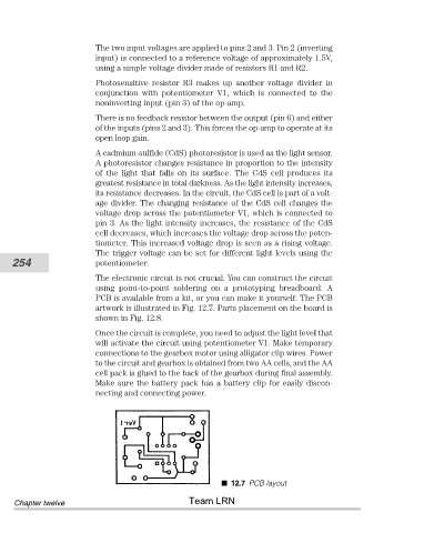
The electronic circuit is not crucial. You can construct the circuit
using point-to-point soldering on a prototyping breadboard. A
PCB is available from a kit, or you can make it yourself. The PCB
artwork is illustrated in Fig. 12.7. Parts placement on the board is
shown in Fig. 12.8.
Once the circuit is complete, you need to adjust the light level that
will activate the circuit using potentiometer V1. Make temporary
connections to the gearbox motor using alligator clip wires. Power
to the circuit and gearbox is obtained from two AA cells, and the AA
cell pack is glued to the back of the gearbox during final assembly.
Make sure the battery pack has a battery clip for easily discon-
necting and connecting power.
12.7 PCB layout
Team LRN
Chapter twelve