
Page 113 - Semiconductor For Micro- and Nanotechnology An Introduction For Engineers
P. 113
The Electronic System
ξ
C
2
2ξ C – ξ 2
-----------------------------
2
2
– tan ξ C – 2ξ
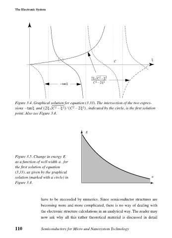
Figure 3.4. Graphical solution for equation (3.33). The intersection of the two expres-
⁄
2
2
2
sions tan– ξ and 2ξ C –( 2 ξ ) ( C – 2ξ ) , indicated by the circle, is the first solution
point. Also see Figure 3.4.
E
Figure 3.5. Change in energy E
a
as a function of well width , for
the first solution of equation
(3.33), as given by the graphical
solution (marked with a circle) in a
Figure 3.4.
have to be succeeded by numerics. Since semiconductor structures are
becoming more and more complicated, there is no way of dealing with
the electronic structure calculations in an analytical way. The reader may
now ask why all this rather theoretical material is discussed in detail
110 Semiconductors for Micro and Nanosystem Technology