Page 167 - Semiconductor For Micro- and Nanotechnology An Introduction For Engineers
P. 167
The Electromagnetic System
⁄
n πxL]
(
[
,
E cos
E xt) =
ωt –
j
0
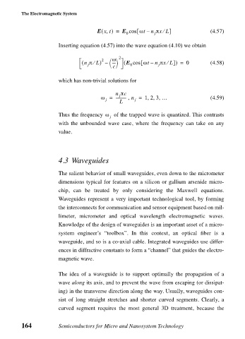
Inserting equation (4.57) into the wave equation (4.10) we obtain (4.57)
ω
2
⁄
( n π L⁄ ) – 2 ( E cos [ ωt – n πxL]) = 0 (4.58)
----
j 0 j
c
which has non-trivial solutions for
n πc
j
,,,
ω = ----------- , n = 123 … (4.59)
j j
L
Thus the frequency ω j of the trapped wave is quantized. This contrasts
with the unbounded wave case, where the frequency can take on any
value.
4.3 Waveguides
The salient behavior of small waveguides, even down to the micrometer
dimensions typical for features on a silicon or gallium arsenide micro-
chip, can be treated by only considering the Maxwell equations.
Waveguides represent a very important technological tool, by forming
the interconnects for communication and sensor equipment based on mil-
limeter, micrometer and optical wavelength electromagnetic waves.
Knowledge of the design of waveguides is an important asset of a micro-
system engineer’s “toolbox”. In this context, an optical fiber is a
waveguide, and so is a co-axial cable. Integrated waveguides use differ-
ences in diffractive constants to form a “channel” that guides the electro-
magnetic wave.
The idea of a waveguide is to support optimally the propagation of a
wave along its axis, and to prevent the wave from escaping (or dissipat-
ing) in the transverse direction along the way. Usually, waveguides con-
sist of long straight stretches and shorter curved segments. Clearly, a
curved segment requires the most general 3D treatment, because the
164 Semiconductors for Micro and Nanosystem Technology

