
Page 79 - Semiconductor For Micro- and Nanotechnology An Introduction For Engineers
P. 79
The Crystal Lattice System
ω k()
k k
Γ ∆ X UK Σ Γ Λ LL K W X
,
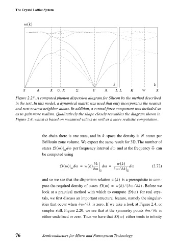
Figure 2.23. A computed phonon dispersion diagram for Silicon by the method described
in the text. In this model, a dynamical matrix was used that only incorporates the nearest
and next nearest neighbor atoms. In addition, a central force component was included so
as to gain more realism. Qualitatively the shape closely resembles the diagram shown in
Figure 2.4, which is based on measured values as well as a more realistic computation.
k
the chain there is one state, and in -space the density is N states per
Brillouin zone volume. We expect the same result for 3D. The number of
ω
states D ω() dω per frequency interval dω and at the frequency can
ω
be computed using
∂k wk()
D ω() dω = wk()------- dω = ----------------------dω (2.72)
⁄
ω ∂ω ∂ω ∂k
ω ω
and so we see that the dispersion relation ω k() is a prerequisite to com-
⁄
⁄
pute the required density of states D ω() = wk() ( ∂ω ∂k) . Before we
look at a practical method with which to compute D ω() for real crys-
tals, we first discuss an important structural feature, namely the singular-
ities that occur when ∂ω ∂k⁄ is zero. If we take a look at Figure 2.4, or
simpler still, Figure 2.20, we see that at the symmetry points ∂ω ∂k⁄ is
either undefined or zero. Thus we have that D ω() either tends to infinity
76 Semiconductors for Micro and Nanosystem Technology