
Page 133 - The Art and Science of Analog Circuit Design
P. 133
Analog Breadboardiog
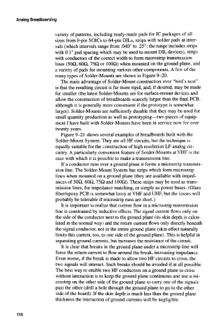
variety of patterns, including ready-made pads for 1C packages of all
sizes from 8-pin SOICs to 64-pin DILs, strips with solder pads at inter-
vals (which intervals range from ,040" to .25"; the range includes strips
with 0.1" pad spacing which may be used to mount DIL devices), strips
with conductors of the correct width to form microstrip transmission
lines (50O, 60H, 75£1 or 100O) when mounted on the ground plane, and
a variety of pads for mounting various other components. A few of the
many types of Solder-Mounts are shown in Figure 9-20.
The main advantage of Solder-Mount construction over "bird's nest"
is that the resulting circuit is far more rigid, and, if desired, may be made
far smaller (the latest Solder-Mounts are for surface-mount devices and
allow the construction of breadboards scarcely larger than the final PCB,
although it is generally more convenient if the prototype is somewhat
larger). Solder-Mounts are sufficiently durable that they may be used for
small quantity production as well as prototyping—two pieces of equip-
ment I have built with Solder-Mounts have been in service now for over
twenty years.
Figure 9-21 shows several examples of breadboards built with the
Solder-Mount System. They are all HF circuits, but the technique is
equally suitable for the construction of high resolution LF analog cir-
cuitry. A particularly convenient feature of Solder-Mounts at VHF is the
ease with which it is possible to make a transmission line.
If a conductor runs over a ground plane it forms a microstrip transmis-
sion line. The Solder-Mount System has strips which form microstrip
lines when mounted on a ground plane (they are available with imped-
ances of 50O, 60H, 75Q and 100H). These strips may be used as trans-
mission lines, for impedance matching, or simply as power buses, (Glass
fiber/epoxy PCB is somewhat lossy at VHF and UHF, but the losses will
probably be tolerable if microstrip runs are short.)
It is important to realize that current flow in a microstrip transmission
line is constrained by inductive effects. The signal current flows only on
the side of the conductor next to the ground plane (its skin depth is calcu-
lated in the normal way) and the return current flows only directly beneath
the signal conductor, not in the entire ground plane (skin effect naturally
limits this current, too, to one side of the ground plane). This is helpful in
separating ground currents, but increases the resistance of the circuit.
It is clear that breaks in the ground plane under a microstrip line will
force the return current to flow around the break, increasing impedance.
Even worse, if the break is made to allow two HF circuits to cross, the
two signals will interact. Such breaks should be avoided if at all possible.
The best way to enable two HF conductors on a ground plane to cross
without interaction is to keep the ground plane continuous and use a mi-
crostrip on the other side of the ground plane to carry one of the signals
past the other (drill a hole through the ground plane to go to the other
side of the board). If the skin depth is much less than the ground plane
thickness the interaction of ground currents will be negligible.
116