
Page 131 - The Art and Science of Analog Circuit Design
P. 131
Analog Breadboarding
temporary structure, designed to test the performance of a circuit or sys-
tem, and must therefore be easy to modify.
There are many commercial breadboarding systems, but almost all
of them are designed to facilitate the breadboarding of digital systems,
where noise immunities are hundreds of millivolts or more, (We shall
discuss the exception to this generality later.) Matrix board (Veroboard,
etc.), wire-wrap, and plug-in breadboard systems (Bimboard, etc.) are,
without exception, unsuitable for high performance or high frequency
analog breadboarding. They have too high resistance, inductance and
capacitance. Even the use of 1C sockets is inadvisable. (All analog engi-
neers should practice the art of unsoldering until they can remove an 1C
from a breadboard [or a plated-through PCB] without any damage to the
board or the device—solder wicks and solder suckers are helpful in ac-
complishing this.)
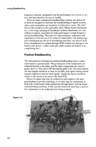
Practical Breadboarding
The most practical technique for analog breadboarding uses a copper-
clad board as a ground plane. The ground pins of the components are
soldered directly to the plane, and the other components are wired to-
gether above it. This allows HF decoupling paths to be very short indeed.
All lead lengths should be as short as possible, and signal routing should
separate high-level and low-level signals. Ideally the layout should be
similar to the layout to be used on the final PCB.
Pieces of copper-clad may be soldered at right angles to the main
ground plane to provide screening, or circuitry may be constructed on
both sides of the board (with connections through holes) with the board
itself providing screening. In this case the board will need legs to protect
the components on the underside from being crushed.
Figure 9-19.
114