
Page 155 - The Art and Science of Analog Circuit Design
P. 155
Car! Battles
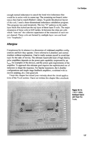
enough mutual inductance to cancel the bond wire inductance that
would-be in series with its center tap. The remaining net branch induc-
tances then had to match Hallen's values. To guide the physical layout
of this coil, I used a three-dimensional inductance calculation program.
This program was used iteratively. The two "G" patterns on the multi-
layer thick film hybrid are the top layer of these input T-coils. The major
dimension of these coils is 0.05 inches. In between the chips are coils
which "tune out" the collector capacitance of the transistor of each out-
put channel. These coils are formed by multiple-layer runs and bond
wire "loopbacks."
Conspicuous by its absence is a discussion of wideband amplifier config-
urations and how they operate. I have referred to f,-doublers and current
doublers without explanation. I had to really restrain myself to avoid that
topic for the sake of brevity. The ultimate bandwidth limit of high-fidelity
pulse amplifiers depends on the power gain capability (expressed by an
r
fMAx» f° example) of the devices, and the power gain requirements of the
amplifier. To approach this ultimate goal requires the sophisticated use of
inductors to shape the response. For bipolar transistors, the f t-doubler
configurations and single-stage feedback amplifiers, combined with in-
ductive peaking, do a very good job.
I hope this chapter has raised your curiosity about the circuit applica-
tions of the T-coil section. I have not written this chapter like a textbook
Figure 10-12.
11A721.5QHZ
MuttRayitr-Hybrid
witi Thick Film
T-coils.
137