
Page 167 - The Art and Science of Analog Circuit Design
P. 167
Jim Williams
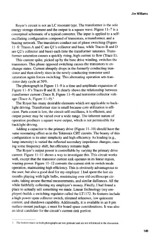
Royer's circuit is not an LC resonant type. The transformer is the sole
energy storage element and the output is a square wave. Figure 11-7 is a
conceptual schematic of a typical converter. The input is applied to a self-
oscillating configuration composed of transistors, a transformer, and a
biasing network. The transistors conduct out of phase switching (Figure
11-8: Traces A and C are Ql's collector and base, while Traces B and D
are Ql's collector and base) each time the transformer saturates. Trans-
former saturation causes a quickly rising, high current to flow (Trace E).
This current spike, picked up by the base drive winding, switches the
transistors. This phase opposed switching causes the transistors to ex-
change states. Current abruptly drops in the formerly conducting tran-
sistor and then slowly rises in the newly conducting transistor until
saturation again forces switching. This alternating operation sets tran-
sistor duty cycle at 50%.
The photograph in Figure 11-9 is a time and amplitude expansion of
Figure 11-8's Traces B and E. It clearly shows the relationship between
transformer current (Trace B, Figure 11-9) and transistor collector volt-
1
age (Trace A, Figure 11-9).
The Royer has many desirable elements which are applicable to back-
light driving. Transformer size is small because core utilization is effi-
cient. Parts count is low, the circuit self-oscillates, it is efficient, and
output power may be varied over a wide range. The inherent nature of
operation produces a square wave output, which is not permissible for
backlight driving.
Adding a capacitor to the primary drive (Figure 11-10) should have the
same resonating effect as in the Tektronix CRT circuits. The beauty of this
configuration is its utter simplicity and high efficiency. As loading (e.g.,
lamp intensity) is varied the reflected secondary impedance changes, caus-
ing some frequency shift, but efficiency remains high.
The Royer's output power is controllable by varying the primary drive
current. Figure 11-11 shows a way to investigate this. This circuit works
well, except that the transistor current sink operates in its linear region,
wasting power. Figure 11-12 converts the current sink to switch mode
operation, maintaining high efficiency. This is obviously advantageous to
the user, but also a good deal for my employer. I had spent the last six
months playing with light bulbs, reminiscing over old oscilloscope cir-
cuits, taking arcane thermal measurements, and similar dalliances. All the
while faithfully collecting my employer's money. Finally, I had found a
place to actually sell something we made. Linear Technology (my em-
ployer) builds a switching regulator called the LT1172. Its features include
a high power open collector switch, trimmed reference, low quiescent
current, arid shutdown capability. Additionally, it is available in an 8 pin
surface-mount package, a must for board space considerations. It was also
an ideal candidate for the circuit's current sink portion.
J The bottom traces in both photographs are not germane and are not referenced in the discussion.
149