
Page 502 - The Mechatronics Handbook
P. 502
0066_frame_C19 Page 124 Wednesday, January 9, 2002 5:32 PM
Evaporated
metal electrodes
Photoresistor Incident
radiation
Bias
voltage Output
R L
voltage
Photoconducting
material
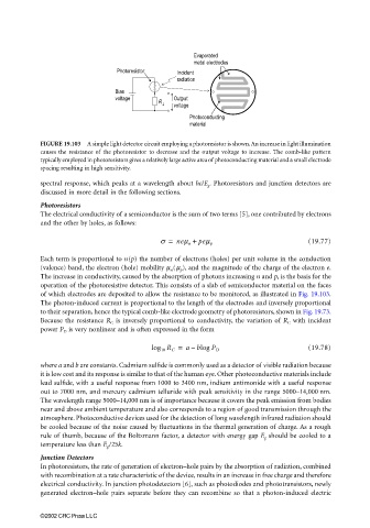
FIGURE 19.103 A simple light detector circuit employing a photoresistor is shown. An increase in light illumination
causes the resistance of the photoresistor to decrease and the output voltage to increase. The comb-like pattern
typically employed in photoresistors gives a relatively large active area of photoconducting material and a small electrode
spacing resulting in high sensitivity.
spectral response, which peaks at a wavelength about hc/E g . Photoresistors and junction detectors are
discussed in more detail in the following sections.
Photoresistors
The electrical conductivity of a semiconductor is the sum of two terms [5], one contributed by electrons
and the other by holes, as follows:
σ = neµ n + peµ p (19.77)
Each term is proportional to n(p) the number of electrons (holes) per unit volume in the conduction
(valence) band, the electron (hole) mobility µ n (µ p ), and the magnitude of the charge of the electron e.
The increase in conductivity, caused by the absorption of photons increasing n and p, is the basis for the
operation of the photoresistive detector. This consists of a slab of semiconductor material on the faces
of which electrodes are deposited to allow the resistance to be monitored, as illustrated in Fig. 19.103.
The photon-induced current is proportional to the length of the electrodes and inversely proportional
to their separation, hence the typical comb-like electrode geometry of photoresistors, shown in Fig. 19.73.
Because the resistance R C is inversely proportional to conductivity, the variation of R C with incident
power P D is very nonlinear and is often expressed in the form
log 10 R C = ablog P D (19.78)
–
where a and b are constants. Cadmium sulfide is commonly used as a detector of visible radiation because
it is low cost and its response is similar to that of the human eye. Other photoconductive materials include
lead sulfide, with a useful response from 1000 to 3400 nm, indium antimonide with a useful response
out to 7000 nm, and mercury cadmium telluride with peak sensitivity in the range 5000–14,000 nm.
The wavelength range 5000–14,000 nm is of importance because it covers the peak emission from bodies
near and above ambient temperature and also corresponds to a region of good transmission through the
atmosphere. Photoconductive devices used for the detection of long wavelength infrared radiation should
be cooled because of the noise caused by fluctuations in the thermal generation of charge. As a rough
rule of thumb, because of the Boltzmann factor, a detector with energy gap E g should be cooled to a
temperature less than E g /25k.
Junction Detectors
In photoresistors, the rate of generation of electron–hole pairs by the absorption of radiation, combined
with recombination at a rate characteristic of the device, results in an increase in free charge and therefore
electrical conductivity. In junction photodetectors [6], such as photodiodes and phototransistors, newly
generated electron–hole pairs separate before they can recombine so that a photon-induced electric
©2002 CRC Press LLC