
Page 503 - The Mechatronics Handbook
P. 503
0066_frame_C19 Page 125 Wednesday, January 9, 2002 5:32 PM
Incident
radiation
+
p silicon
Metal contact
Symbol
Insulation _ _ _ _ _ _ _ _ _ _ _
+ + + + + + + + + + +
Depletion n silicon
region
+
n silicon
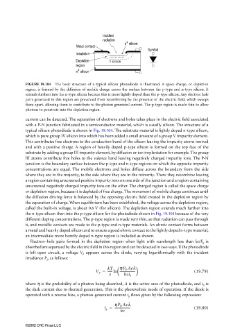
FIGURE 19.104 The basic structure of a typical silicon photodiode is illustrated. A space charge, or depletion
region, is formed by the diffusion of mobile charge across the surface between the p-type and n-type silicon. It
extends furthest into the n-type silicon because this is more lightly doped than the p-type silicon. Any electron hole
pairs generated in this region are prevented from recombining by the presence of the electric field, which sweeps
them apart, allowing them to contribute to the photon generated current. The p-type region is made thin to allow
photons to penetrate into the depletion region.
current can be detected. The separation of electrons and holes takes place in the electric field associated
with a P-N junction fabricated in a semiconductor material, which is usually silicon. The structure of a
typical silicon photodiode is shown in Fig. 19.104. The substrate material is lightly doped n-type silicon,
which is pure group IV silicon into which has been added a small amount of a group V impurity element.
This contributes free electrons to the conduction band of the silicon leaving the impurity atoms ionized
and with a positive charge. A region of heavily doped p-type silicon is formed on the top face of the
substrate by adding a group III impurity element, by diffusion or ion implantation for example. The group
III atoms contribute free holes to the valence band leaving negatively charged impurity ions. The P-N
junction is the boundary surface between the p-type and n-type regions on which the opposite impurity
concentrations are equal. The mobile electrons and holes diffuse across the boundary from the side
where they are in the majority, to the side where they are in the minority. There they recombine leaving
a region containing unscreened positive impurity ions on one side of the junction and a region containing
unscreened negatively charged impurity ions on the other. The charged region is called the space charge
or depletion region, because it is depleted of free charge. The movement of mobile charge continues until
the diffusion driving force is balanced by the opposing electric field created in the depletion region by
the separation of charge. When equilibrium has been established, the voltage across the depletion region,
called the built-in voltage, is about 0.6 V (for silicon). The depletion region extends much further into
the n-type silicon than into the p-type silicon for the photodiode shown in Fig. 19.104 because of the very
different doping concentrations. The p-type region is made very thin, so that radiation can pass through
it, and metallic contacts are made to the p-type and n-type materials. An ohmic contact forms between
a metal and heavily doped silicon and to ensure a good ohmic contact to the lightly doped n-type material,
an intermediate more heavily doped n-type region is included as shown.
Electron–hole pairs formed in the depletion region when light with wavelength less than hc/E g is
absorbed are separated by the electric field in this region and can be detected in two ways. If the photodiode
is left open circuit, a voltage V p appears across the diode, varying logarithmically with the incident
irradiance P D as follows:
V p = kT ηP D Aeλ (19.79)
--------------------
------ln
e hci 0
where η is the probability of a photon being absorbed, A is the active area of the photodiode, and i 0 is
the dark current due to thermal generation. This is the photovoltaic mode of operation. If the diode is
operated with a reverse bias, a photon-generated current i p flows given by the following expression:
ηP D Aeλ
i p = -------------------- (19.80)
hc
©2002 CRC Press LLC