
Page 508 - The Mechatronics Handbook
P. 508
0066_frame_C19 Page 130 Wednesday, January 9, 2002 5:32 PM
Gate
electrode
Phase 3
Phase 2
Phase 1
Insulating layer
Potential
well P-type silicon substrate
1/3 cycle
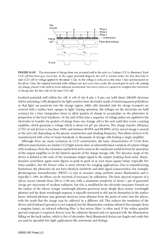
FIGURE 19.107 The movement of charge from one potential well to the next in a 3-phase CCD is illustrated. Each
CCD cell has three gate electrodes. In the upper potential diagram, the well is formed under the first electrode in
each CCD cell by voltage applied to the phase 1 line. As the voltage is reduced on the phase 1 line and increased on
the phase 2 line, the original potential wells collapse and new ones form under the second gate in each cell, causing
any charge present in the wells to move sideways as indicated. Two more cycles are required to complete the movement
of charge into the first well of the next CCD cell.
localized potential well within the cell. A cell of size 8 µm × 8 µm can hold about 200,000 electrons
before saturating. Cells designed to be light sensitive have electrodes made of semitransparent polysilicon
so that light can penetrate into the storage region, while cells intended only for charge transport are
covered with a surface layer opaque to light. During operation, the voltages on the electrodes are held
constant for a time (integration time) to allow packets of charge to accumulate on the photosites in
proportion to the local irradiance. At the end of this time a sequence of voltage pulses are applied to the
electrodes to transfer the packets of charge from one storage cell to the next until they reach a sensing
amplifier, which generates a voltage which is about 0.6 µV per electron. The charge transfer efficiency
(CTE) of real devices is less than 100% and between 99.95% and 99.999% of the stored charge is moved
to the next cell, depending on the precise construction and clocking frequency. This allows devices to be
manufactured with a line of many hundreds or thousands of storage cells feeding a single amplifier.
Although there are many variations in CCD construction, the basic characteristics of CCDs from
different manufactures are similar. CCD light sensors have an inherently linear variation of output voltage
with irradiance, from the minimum useful level set by noise to the maximum useful level set by saturation
of the output amplifier or by the limited capacity of the charge storage cells. The dynamic range of the
device is defined as the ratio of the maximum output signal to the output resulting from noise. Manu-
facturers sometimes quote noise figures as peak-to-peak or as root-mean-square values (typically five
times smaller), but the former value is more relevant for imaging applications. Due to manufacturing
limitations, the photosites do not have identical sensitivity and dark signal characteristics. For example,
photoresponse nonuniformity (PRNU) is easy to measure using uniform sensor illumination and is
typically 5–10%. Its effects can be removed, if necessary, by calibration. The basic spectral response of a
silicon sensor extends from 200 to 1100 nm, with a maximum sensitivity of about 1 µA of generated
charge per microwatt of incident radiation, but this is modified by the electrode structures formed on
the surface of the silicon. Longer wavelength photons penetrate more deeply than shorter wavelength
photons and the short wavelength response is typically worsened to 450 nm by absorption in the surface
layers. Infrared photons may generate electrons some distance from the point of entry into the silicon,
with the result that the charge may be collected by a different cell. This reduces the resolution of the
device and if infrared operation is not required, but the illumination contains infrared (for example, from
a tungsten lamp), an infrared reflecting filter (a hot-mirror filter) is often used. If the widest possible
spectral response is required, devices have the substrate thinned and are operated with the illumination
falling on the back surface, which is free of electrodes. Back illuminated devices are fragile and costly but
are used in specialist low-light applications like astronomy and biology.
©2002 CRC Press LLC