
Page 511 - The Mechatronics Handbook
P. 511
0066_frame_C19 Page 133 Wednesday, January 9, 2002 5:32 PM
the image sensing area and increasing aliasing effects compared with frame-transfer sensors. For the
latter, the fill factor, which is the percentage of the imaging area which is light sensitive, can be close to
100% whereas it is usually less than 50% for interline-transfer devices. Localized bright objects tend to
produce vertical streaks in an ILT device because strong light can leak under the narrow light shield
covering the vertical shift registers, causing image smearing similar to that in a full frame device. For
interlaced operation, two adjacent pixels, for example, 1 and 2, 3 and 4, etc. are transferred to a single
shift register cell on one field and in the next field pixels 2 and 3, 4 and 5, etc. are transferred together.
This is rather similar to the interlaced operation of a frame transfer CCD. Many companies manufacture
ILT CCD sensors and cameras including, Hitachi, NEC, Panasonic, Pulnix, and Sony.
CMOS Sensors
CMOS image sensors are based on a technology that is older than CCD technology [12]. However, CCD
sensors originally offered better image quality than CMOS devices could match so they came to dominate
the market. There is now renewed interest in the older technology because it potentially offers major
advantages over CCDs. The CMOS process used in sensors is similar to that which has been highly
developed in order to manufacture dynamic RAM and consequently should be able to produce cheap,
small high-resolution, randomly addressed, low-power sensors. It is also possible to integrate image
sensing, control, processing, and interfacing on the same chip, so that a camera on a chip is possible using
CMOS technology, but not with CCD technology. As a result of recent research and development, several
manufacturers are now claiming to have achieved CMOS sensors providing similar quality to that of
mainstream CCDs. Manufacturers producing CMOS sensors include Fillfactory, National Semiconductor,
Philips, ST Microelectronics, and Y Media.
A CMOS sensor consists of an array of photodiodes, which are connected to readout amplifiers by
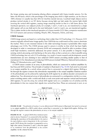
bus lines and MOS switches. The principle of readout is illustrated in Fig. 19.109. Each pixel is connected
to an output amplifier by a switch whose control line is connected to a digital shift register. Shifting a
bit through the register connects the photodiodes sequentially to the output amplifier. Random readout
of the photodiodes can be achieved by replacing the shift register by an address decoder connected to an
address bus. Two-dimensional arrays of photodiodes are connected in a configuration similar to a cross-
point switching matrix with a switch and diode at each cross point and separate vertical and horizontal
shift registers. To scan the array, the vertical shift register turns on a complete row of switches and the
photodiodes in that row output their signals into vertical bus lines. These are connected, in turn, to an
Digital shift register
Amplifier
MOS
switch
Photodiode
FIGURE 19.109 The principle of readout in a one-dimensional CMOS sensor is illustrated. Each pixel is connected
to an output amplifier by a MOS switch whose control line is connected to the digital shift register. Shifting a bit
through the register connects the photodiodes, in turn, to the output amplifier.
FIGURE 19.110 A typical CMOS three-transistor active V dd
pixel is shown. Transistor T 1 is connected to the reset line Reset
Row select
allowing the capacitance of the photodiode to be reset at
T 1
the start of photo-current integration. In the continuous
T
mode CMOS device this transistor is connected to act as 2
Photodiode
high value resistor. Transistors T 2 and T 3 allow the signal T 3
to be transferred from the photodiode to the column Column
amplifier, via the column bus line. bus
©2002 CRC Press LLC