
Page 510 - The Mechatronics Handbook
P. 510
0066_frame_C19 Page 132 Wednesday, January 9, 2002 5:32 PM
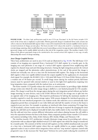
Full frame Frame transfer Interline transfer
CCD CCD CCD
Photosite Horizontal Readout Covered Photosite Vertical shift
shift amplifier storage register
register area
FIGURE 19.108 The three basic architectures used in area CCDs are illustrated. In the full-frame transfer CCD
most of the device area is employed as photosites. Photon-generated charge is transferred down each column one
cell at a time into the horizontal shift register where it must all be transferred to the readout amplifier before another
vertical movement of charge can take place. The frame-transfer CCD reduces the need for a mechanical shutter to
prevent charge smearing, which would otherwise occur, by providing a covered storage area into which all the photon-
generated charge can be rapidly shifted vertically at the end of the integration period. The interline-transfer CCD
allows all the photon-generated charge to be transferred to the covered vertical shift registers in one step, virtually
eliminating this source of charge smearing.
Area Charge-Coupled Devices
Three basic architectures are used in area CCDs and are illustrated in Fig. 19.108. The full-frame CCD
consists of an imaging area separated from a horizontal CCD shift register by a transfer gate. In the
imaging area each photosite is one stage of a vertical shift register separated from neighboring shift
registers by channel stops and anti-blooming structures. During the light integration period, the vertical
clocks are stopped and the photosites collect photoelectrons. At the end of this period the charge is
clocked out vertically, one row at a time into the horizontal shift register. The charge in the horizontal
shift register is then very rapidly shifted towards the output amplifier by the application of a horizontal
clock signal. For example, the RA1001J, 1024 × 1024 pixel full-frame CCD from EG&G Reticon achieves
a readout rate of 30 frames per second. To avoid image smear during the readout period, full-frame
sensors must be operated with external shutters or used in low-light level applications requiring very
long integration times compared with the readout time, as in astronomy.
The frame-transfer CCD greatly reduces the need for an external shutter by providing a light-shielded
storage section into which the entire image charge is shifted at a rate limited primarily by CTE consider-
ations. The charge is read from the storage region during the next integration period without any further
image smearing. In some devices, such as the EG&G Reticon RA1102, the storage area is split into two
on opposite sides of the imaging area. This improves performance by halving the maximum number of
transfers required to reach the nearest storage region. With sensors designed for interlaced operation, as
opposed to the non-interlaced progressive scan readout mode, this reduction occurs automatically. Each
integration period then corresponds to one video field and only half the number of rows in the frame is
required at any one time. For example, to produce an interlaced video frame containing 576 image lines
(CCIR standard), a frame transfer sensor with only 288 rows of storage is required. By changing the clock
signals, the odd field can be displaced vertically by half a line width relative to the even field. This ensures
that the odd and even lines contain different information and reduces aliasing because the cell width is
twice the separation between the lines in the frame. Many companies produce frame-transfer CCD sensors
and cameras including Cohu, Dalsa, EG&G Reticon, EEV, Kodak, Philips, and Thomson-CSF.
The interline-transfer (ILT) architecture virtually eliminates image smear by providing each column
of photosites with an adjacent light-shielded vertical CCD shift register into which the charge is transferred
by a transfer pulse. The contents of all the vertical shift registers are then shifted simultaneously one pixel
at a time into a horizontal shift register where they are rapidly shifted to an output amplifier. This
approach makes it easy to achieve short integration times and true “stop-motion” exposure control with
progressive scan. It also increases the “dead space” between the active pixels reducing the sensitivity of
©2002 CRC Press LLC