
Page 118 - Understanding Automotive Electronics
P. 118
2735 | CH 4 Page 105 Tuesday, March 10, 1998 11:06 AM
MICROCOMPUTER INSTRUMENTATION AND CONTROL 4
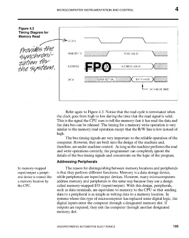
Figure 4.3
Timing Diagram for
Memory Read
FPO
Refer again to Figure 4.3. Notice that the read cycle is terminated when
the clock goes from high to low during the time that the read signal is valid.
This is the signal the CPU uses to tell the memory that it has read the data and
the data bus can be released. The timing for a memory write operation is very
similar to the memory read operation except that the R/W line is low instead of
high.
The bus timing signals are very important to the reliable operation of the
computer. However, they are built into the design of the machine and,
therefore, are under machine control. As long as the machine performs the read
and write operations correctly, the programmer can completely ignore the
details of the bus timing signals and concentrate on the logic of the program.
Addressing Peripherals
In memory-mapped The reason for distinguishing between memory locations and peripherals
input/output a periph- is that they perform different functions. Memory is a data storage device,
eral device is treated like while peripherals are input/output devices. However, many microcomputers
a memory location by address memory and peripherals in the same way because they use a design
the CPU. called memory-mapped I/O (input/output). With this design, peripherals,
such as data terminals, are equivalent to memory to the CPU so that sending
data to a peripheral is as simple as writing data to a memory location. In
systems where this type of microcomputer has replaced some digital logic, the
digital inputs enter the computer through a designated memory slot. If
outputs are required, they exit the computer through another designated
memory slot.
UNDERSTANDING AUTOMOTIVE ELECTRONICS 105