
Page 152 - A Comprehensive Guide to Solar Energy Systems
P. 152
Chapter 8 • Photovoltaics: The Basics 153
−W g
np = n i 2 = BT exp kT , (8.4) 3
3
00
n 0 p 0 =ni2=BT exp−WgkT,
where n i is the so-called intrinsic concentration and B is a characteristic material constant.
In real semiconductors, there exist some impurities or defects, from which electron may
be liberated (donors) or which may generate free holes (acceptors) by overcoming a lower
energy barrier than W g . At room temperature, free carrier concentration is controlled by
those impurity concentrations, donor concentration N D and acceptor concentration N A .
2
p = n / n 0 .
If N D > N A (n-type semiconductor), electron concentration n 0 = N D − N A i n 0 =ND−NA≫p=ni2/n 0
n = n / p 0. The
2
If N A > N D (P-type semiconductor), hole concentration p 0 = N A − N D i p 0 =NA−ND≫n=ni2/p 0
control of free carrier concentration in thermal equilibrium by doping with suitable im-
purities is one of fundamental features of semiconductor technology [1,2]. At thermal
equilibrium, free electrons occupy states with energy close to the bottom of conductive
band; the holes occupy states close to the top of the valence band (in dependence on the
band structure).
8.2.1 Carrier Generation
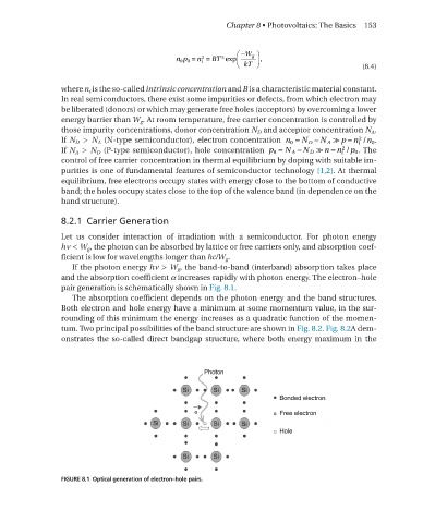
Let us consider interaction of irradiation with a semiconductor. For photon energy
hν < W g , the photon can be absorbed by lattice or free carriers only, and absorption coef-
ficient is low for wavelengths longer than hc/W g .
If the photon energy hν > W g , the band-to-band (interband) absorption takes place
and the absorption coefficient α increases rapidly with photon energy. The electron–hole
pair generation is schematically shown in Fig. 8.1.
The absorption coefficient depends on the photon energy and the band structures.
Both electron and hole energy have a minimum at some momentum value, in the sur-
rounding of this minimum the energy increases as a quadratic function of the momen-
tum. Two principal possibilities of the band structure are shown in Fig. 8.2. Fig. 8.2A dem-
onstrates the so-called direct bandgap structure, where both energy maximum in the
FIGURE 8.1 Optical generation of electron–hole pairs.