
Page 259 - A Comprehensive Guide to Solar Energy Systems
P. 259
262 A COmPreHenSIVe GuIde TO SOlAr enerGy SySTemS
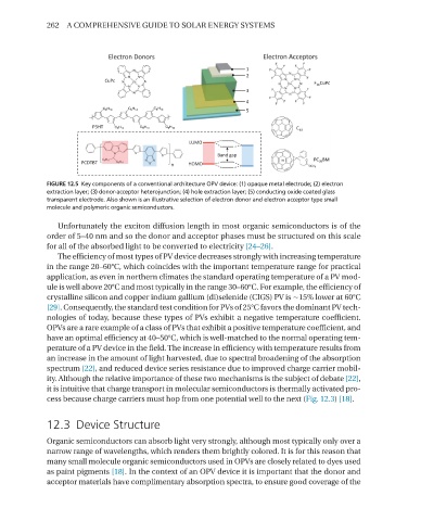
FIGURE 12.5 Key components of a conventional architecture OPV device: (1) opaque metal electrode; (2) electron
extraction layer; (3) donor-acceptor heterojunction; (4) hole extraction layer; (5) conducting oxide coated glass
transparent electrode. Also shown is an illustrative selection of electron donor and electron acceptor type small
molecule and polymeric organic semiconductors.
unfortunately the exciton diffusion length in most organic semiconductors is of the
order of 5–40 nm and so the donor and acceptor phases must be structured on this scale
for all of the absorbed light to be converted to electricity [24–26].
The efficiency of most types of PV device decreases strongly with increasing temperature
in the range 20–60°C, which coincides with the important temperature range for practical
application, as even in northern climates the standard operating temperature of a PV mod-
ule is well above 20°C and most typically in the range 30–60°C. For example, the efficiency of
crystalline silicon and copper indium gallium (di)selenide (CIGS) PV is ∼15% lower at 60°C
[29]. Consequently, the standard test condition for PVs of 25°C favors the dominant PV tech-
nologies of today, because these types of PVs exhibit a negative temperature coefficient.
OPVs are a rare example of a class of PVs that exhibit a positive temperature coefficient, and
have an optimal efficiency at 40–50°C, which is well-matched to the normal operating tem-
perature of a PV device in the field. The increase in efficiency with temperature results from
an increase in the amount of light harvested, due to spectral broadening of the absorption
spectrum [22], and reduced device series resistance due to improved charge carrier mobil-
ity. Although the relative importance of these two mechanisms is the subject of debate [22],
it is intuitive that charge transport in molecular semiconductors is thermally activated pro-
cess because charge carriers must hop from one potential well to the next (Fig. 12.3) [18].
12.3 Device Structure
Organic semiconductors can absorb light very strongly, although most typically only over a
narrow range of wavelengths, which renders them brightly colored. It is for this reason that
many small molecule organic semiconductors used in OPVs are closely related to dyes used
as paint pigments [18]. In the context of an OPV device it is important that the donor and
acceptor materials have complimentary absorption spectra, to ensure good coverage of the