
Page 260 - A Comprehensive Guide to Solar Energy Systems
P. 260
Chapter 12 • Organic Photovoltaics 263
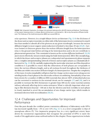
FIGURE 12.6 Schematic illustration of a bilayer (A) and bulk heterojunction (B) OPV device architecture. The thickness
of the organic heterojunction in a bilayer device architecture is constrained to <80 nm by the exciton diffusion bottle
neck. The thickness of the bulk-heterojunction (BHJ) can exceed 300 nm.
solar spectrum. However, in a simple bilayer device architecture (Fig. 12.6) the thickness of
the donor and acceptor materials on either side of the heterojunction is constrained to much
less than needed to absorb all of the photons at any given wavelength, because the exciton
diffusion length in most organic semiconductors is limited to less than 40 nm [25,26]. exci-
tons formed at distances greater than the exciton diffusion length from the heterojunction
relax to the ground state before arriving at the heterojunction and so do not contribute to
photocurrent generation. This constraint is known as the exciton diffusion bottleneck [25,26]
and is most effectively circumvented using the bulk-heterojunction (BHJ) film morphology,
in which the donor and acceptor phases are codeposited and spontaneously phase separate
into a complex interpenetrating network of donor and acceptor phases as schematically il-
lustrated in Fig. 12.6B. By carefully engineering the molecular structure and film deposition
conditions it is possible to ensure that the dimensions of both phases are comparable to
twice the exciton diffusion length, and so all excitons formed throughout the thickness of
the films are within one exciton diffusion length of a heterojunction. despite the complexity
of this layer, it works remarkably well given that free charge carriers must move along narrow
winding tracks of each phase to the electrodes without recombining. remarkably, it has now
been shown for a number of different BHJ materials that almost 100% of absorbed photons
can be converted to excitons in the external circuit; see for example [27] and [28], and it is
possible to increase the BHJ thicknesses to greater than 300 nm for some material systems
without adversely affecting device series resistance. What is critically important when scal-
ing to film thickness beyond ∼100 nm is that the electron and hole mobility in each phase
is closely matched to avoid the accumulation of one charge carrier type, which results in
increased electron-hole recombination [30,31].
12.4 Challenges and Opportunities for Improved
Performance
Over the past decade the certified power conversion efficiency of laboratory scale OPVs
has increased rapidly from ∼3% to over 13% (Fig. 12.7), to a level comparable to that of
amorphous silicon PV. This impressive progress has, to a very significant extent, been
driven by commercial organizations that recognize the potential of OPVs to meet the
needs of the application areas outlined earlier in this chapter. These organizations include