
Page 265 - A Comprehensive Guide to Solar Energy Systems
P. 265
268 A COmPreHenSIVe GuIde TO SOlAr enerGy SySTemS
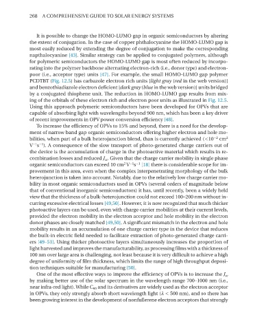
It is possible to change the HOmO-lumO gap in organic semiconductors by altering
the extent of conjugation. In the case of copper phthalocyanine the HOmO-lumO gap is
most easily reduced by extending the degree of conjugation to make the corresponding
napthalocyanine [43]. Similar strategy can be applied to conjugated polymers, although
for polymeric semiconductors the HOmO-lumO gap is most often reduced by incorpo-
rating into the polymer backbone alternating electron-rich (i.e., donor type) and electron-
poor (i.e., acceptor type) units [47]. For example, the small HOmO-lumO gap polymer
PCdTBT (Fig. 12.5) has carbazole electron rich units [light gray (red in the web version)]
and benzothiadiazole electron deficient [dark gray (blue in the web version)] units bridged
by a conjugated thiophene unit. The reduction in HOmO-lumO gap results from mix-
ing of the orbitals of these electron rich and electron poor units as illustrated in Fig. 12.5.
using this approach polymeric semiconductors have been developed for OPVs that are
capable of absorbing light with wavelengths beyond 900 nm, which has been a key driver
of recent improvements in OPV power conversion efficiency [48].
To increase the efficiency of OPVs to 15% and beyond, there is a need for the develop-
ment of narrow band gap organic semiconductors offering higher electron and hole mo-
2
−2
bilities, when part of a bulk heterojunction blend, than is currently achieved (<10 cm
−1 −1
V s ). A consequence of the slow transport of photo-generated charge carriers out of
the device is the accumulation of charge in the photoactive material which results in re-
combination losses and reduced J sc . Given that the charge carrier mobility in single phase
2
−1 −1
organic semiconductors can exceed 10 cm V s [18] there is considerable scope for im-
provement in this area, even when the complex interpenetrating morphology of the bulk
heterojunction is taken into account. notably, due to the relatively low charge carrier mo-
bility in most organic semiconductors used in OPVs (several orders of magnitude below
that of conventional inorganic semiconductors) it has, until recently, been a widely held
view that the thickness of a bulk-heterojunction could not exceed 100–200 nm without in-
curring excessive electrical losses [49,50]. However, it is now recognized that much thicker
photoactive layers can be used, even with charge carrier mobilities at their current levels,
provided the electron mobility in the electron acceptor and hole mobility in the electron
donor phases are closely matched [49,50]. A significant mismatch in the electron and hole
mobility results in an accumulation of one charge carrier type in the device that reduces
the built-in electric field needed to facilitate extraction of photo-generated charge carri-
ers [49–51]. using thicker photoactive layers simultaneously increases the proportion of
light harvested and improves the manufacturability, as processing films with a thickness of
100 nm over large area is challenging, not least because it is very difficult to achieve a high
degree of uniformity of film thickness, which limits the range of high throughput deposi-
tion techniques suitable for manufacturing [50].
One of the most effective ways to improve the efficiency of OPVs is to increase the J sc
by making better use of the solar spectrum in the wavelength range 700–1000 nm (i.e.,
near infra-red light). While C 60 and its derivatives are widely used as the electron acceptor
in OPVs, they only strongly absorb short wavelength light (λ < 500 nm), and so there has
been growing interest in the development of nonfullerene electron acceptors that strongly