
Page 46 - Analog Circuit Design Art, Science, and Personalities
P. 46
Bernard Gordon
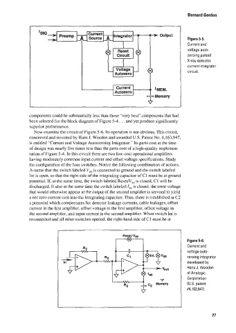
Figure 5-5.
Current and
voltage auto-
zeroing pulsed
X-ray detector
current integrator
circuit.
components could be substantially less than those “very best” components thar had
been selected for the block diagram of Figure 5-4 . . . and yet produce signilicantly
superior performance.
Now examine the circuit of Figure 5-6. Its operation is not obvious. This circuit,
conceived and invented by Hans J. Weedon and awarded U.S. Patent No. 4,163,947,
is entitled “Current and Voltage Autozeroing Integrator.” Its parts cost at the time
of design was nearly five times less than the parts cost of a high-quality implemen-
tation of Figure 5-4. In this circuit there are two low-cost operational amplifiers
having moderately common input current and offset voltage specifications. Study
thc configuration of‘the four switches. Notice the following combination of actions.
Assume that the switch labeled Viz is connected to ground and the switch labeled
Int. is open, so that the right side of the integrating capacitor of C1 must be at ground
potential. If, at the same time, the switch labeled Reset/V,, is closed, C1 will bc
discharged. If‘ also at the same time the switch labeled I,, is closed, the error voltage
that would otherwise appear at the output of the second amplifier is servoed to yield
a nct zero currcnt sum into the integrating capacitor. Thus, there is established at C2
a potential which compensates for detector leakage currents, cable leakages, offset
current in the first amplifier, offset voltage in the first amplifier, offset voltage in
the second amplifier, and input current in the second amplifier. When switch In1 is
rec:onnected and all other switches opened. the right-hand side of Cl must be at
Figure 5-6.
Current and
voltage auto-
zeroing integrator
developed by
Hans J. Weeaon
of halogic
Corporation
(US. patent
#4.163,947).
27