
Page 343 - Analog and Digital Filter Design
P. 343
340 Analog and Digital Filter Design
SWI sw2
I
t"
II II II
CLOSED
OPEN
SWITCH 2
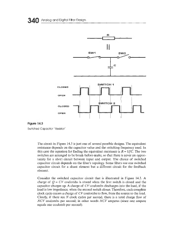
Figure 14.3
Switched Capacitor "Resistor"
The circuit in Figure 14.3 is just one of several possible designs. The equivalent
resistance depends on the capacitor value and the switching frequency used. In
this case the equation for finding the equivalent resistance is R = 1yC. The two
switches are arranged to be break-before-make, so that there is never an oppor-
tunity for a short circuit between input and output. The choice of switched
capacitor circuit depends on the filter's topology. Some filters use one switched
capacitor circuit for a shunt element but a different circuit for the feedback
element.
Consider the switched capacitor circuit that is illustrated in Figure 14.3. A
charge of (2 = CV coulombs is stored when the first switch is closed and the
capacitor charges up. A charge of CVcoulombs discharges into the load, if the
load is low impedance, when the second switch closes. Therefore, each complete
clock cycle causes a charge of CVcoulombs to flow, from the source to the load.
Clearly, if there are N clock cycles per second, there is a total charge flow of
NCV coulombs per second; in other words NCV amperes (since one ampere
equals one coulomb per second).