
Page 178 - Bebop to The Boolean Boogie An Unconventional Guide to Electronics Fundamentals, Components, and Processes
P. 178
Integrated Circuits (ICs) 159
With devices whose geometries were 1 pm and
higher, it was relatively easy to talk about them in
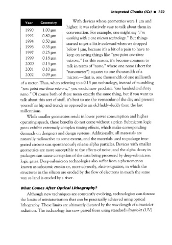
1990 1.00 pm conversation. For example, one might say “I’m
1992 0.80 pm working with a one micron technology. ” But things
1991 0.50 pm started to get a little awkward when we dropped
1996 0.35 pm below 1 pm, because it’s a bit of a pain to have to
1999 0.25 pm keep on saying things like “zero point one-three
1999 0.18 pm microns.” For this reason, it’s become common to
2000 0.13 pm talk in terms of “nano,” where one nano (short for
2001 0.10 pm “nanometer”) equates to one thousandth of a
2002 0.09 pm
micron-that is, one thousandth of one millionth
of a meter. Thus, when referring to a 0.13 pm technology, instead of mumbling
“zero point one-three microns,” you would now proclaim “one hundred and thirty
nuno.” Of course both of these mean exactly the same thing, but if you want to
talk about this sort of stuff, it’s best to use the vernacular of the day and present
yourself as hip and trendy as opposed to an old fuddy-duddy from the last
millennium.
While smaller geometries result in lower power consumption and higher
operating speeds, these benefits do not come without a price. Submicron logic
gates exhibit extremely complex timing effects, which make corresponding
demands on designers and design systems. Additionally, all materials are
naturally radioactive to some extent, and the materials used to package inte-
grated circuits can spontaneously release alpha particles. Devices with smaller
geometries are more susceptible to the effects of noise, and the alpha decay in
packages can cause corruption of the data being processed by deep-submicron
logic gates. Deep-submicron technologies also suffer from a phenomenon
known as subatomic erosion or, more correctly, electromigration, in which the
structures in the silicon are eroded by the flow of electrons in much the same
way as land is eroded by a river.
What Comes After Optical Lithography?
Although new techniques are constantly evolving, technologists can foresee
the limits of miniaturization that can be practically achieved using optical
lithography. These limits are ultimately dictated by the wavelength of ultraviolet
radiation. The technology has now passed from using standard ultraviolet (UV)