
Page 173 - Bebop to The Boolean Boogie An Unconventional Guide to Electronics Fundamentals, Components, and Processes
P. 173
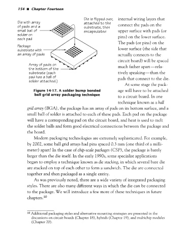
154    Chapter Fourteen


                                              Die is flipped over,   internal wiring layers that
                                              attached to the    connect the pads on the
                                              substrate, then
                                                                 upper surface with pads (or
                                                                 pins) on the lower surface.
                                                                 The pads (or pins) on the
                                                                 lower surface (the side that
                                                                 actually connects to the
                                                                 circuit board) will be spaced
                                                                 much father apart-rela-
                 substrate (each                                 tively speaking-than   the
                 pad has a ball of                              pads that connect to the die.
                 solder attached.)
                                                                    At some stage the pack-
                   Figure 14-1 7. A solder bump bonded           age will have to be attached
                    ball grid array packaging technique          to a circuit board. In one
                                                                 technique known as a bull

                grid array (BGA) , the package has an array of pads on its bottom surface, and a
                small ball of solder is attached to each of these pads. Each pad on the package
                will have a corresponding pad on the circuit board, and heat is used to melt
                the solder balls and form good electrical connections between the package and
                the board.
                   Modern packaging technologies are extremely sophisticated. For example,
                by 2002, some ball grid arrays had pins spaced 0.3 mm (one third of a milli-
                meter) apart! In the case of chip-scale packages (CSP), the package is barely
                larger than the die itself. In the early 1990s, some specialist applications
                began to employ a technique known as die stacking, in which several bare die
                are stacked on top of  each other to form a sandwich. The die are connected
                together and then packaged as a single entity.
                   As was previously noted, there are a wide variety of  integrated packaging
                styles. There are also many different ways in which the die can be connected
                to the package. We will introduce a few more of these techniques in future
                chapters.  lo


                10 Additional packaging styles and alternative mounting strategies are presented in the
                  discussions on circuit boards (Chapter 18), hybrids (Chapter 19), and multichip modules
                  (Chapter 20).