
Page 170 - Bebop to The Boolean Boogie An Unconventional Guide to Electronics Fundamentals, Components, and Processes
P. 170
Integrated Circuits (ICs) 151
The Packaging Process
The individual integrated circuits are tested while they are still part of the
wafer in a process known as wafer probing. An automated tester places probes on
the device’s pads, applies power to the power pads, injects a series of signals
into the input pads, and monitors the corresponding signals returned from the
output pads. Each integrated circuit is tested in turn, and any device that fails
the tests is automatically tagged with a splash of dye for subsequent rejection.
The yield is the number of devices that pass
tests as a percentage of the total number
fabricated on that wafer.
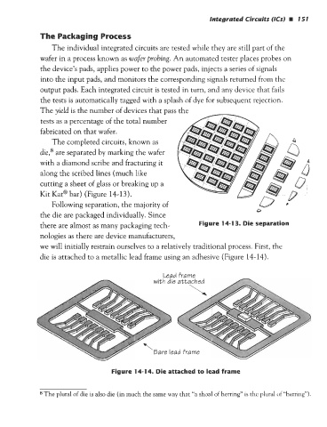
The completed circuits, known as
die,s are separated by marking the wafer
with a diamond scribe and fracturing it
along the scribed lines (much like
cutting a sheet of glass or breaking up a
Kit Kat@ bar) (Figure 14-13).
Following separation, the majority of
the die are packaged individually. Since
there are almost as many packaging tech- Figure 14-1 3. Die separation
nologies as there are device manufacturers,
we will initially restrain ourselves to a relatively traditional process. First, the
die is attached to a metallic lead frame using an adhesive (Figure 14-14).
Lead frame
Bare lead frame
Figure 14-14. Die attached to lead frame
8 The plural of die is also die (in much the same way that “a shoal of herring” is the plural of “herring”).