
Page 169 - Bebop to The Boolean Boogie An Unconventional Guide to Electronics Fundamentals, Components, and Processes
P. 169
150 Chapter Fourteen
of transistors increased, engineers required more and more tracking layers.
The problem is that when a layer of insulating silicon dioxide is deposited
over a tracking layer, you end up with slight “bumps” where the tracks are
(like snow falling over a snoozing polar bear-you end up with a bump).
After a few tracking layers, the bumps are pronounced enough that you
can’t continue. The answer is to re-planarize the wafer (smooth the bumps out)
after each tracking and silicon dioxide layer combo has been created. This is
achieved by means of a process called chemical mechanical polishing (CMP),
which returns the wafer to a smooth, flat surface before the next tracking layer
is added. With manufacturers using this process, high-end silicon chips could
support up to eight tracking layers by 2002.
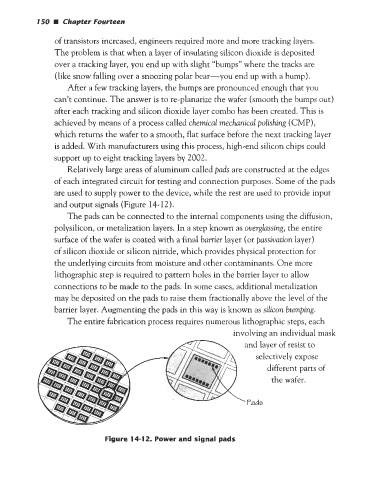
Relatively large areas of aluminum called pads are constructed at the edges
of each integrated circuit for testing and connection purposes. Some of the pads
are used to supply power to the device, while the rest are used to provide input
and output signals (Figure 14- 12).
The pads can be connected to the internal components using the diffusion,
polysilicon, or metalization layers. In a step known as ouerglassing, the entire
surface of the wafer is coated with a final barrier layer (or passivation layer)
of silicon dioxide or silicon nitride, which provides physical protection for
the underlying circuits from moisture and other contaminants. One more
lithographic step is required to pattern holes in the barrier layer to allow
connections to be made to the pads. In some cases, additional metalization
may be deposited on the pads to raise them fractionally above the level of the
barrier layer. Augmenting the pads in this way is known as silicon bumping.
The entire fabrication process requires numerous lithographic steps, each
involving an individual mask
and layer of resist to
selectively expose
different parts of
the wafer.
Pads
Figure 14-12. Power and signal pads