
Page 164 - Bebop to The Boolean Boogie An Unconventional Guide to Electronics Fundamentals, Components, and Processes
P. 164
Integrated Circuits (ICs) 145
single integrated circuit, which is typically in the region of lmm x lmm to
lOmm x lOmm, but may be even larger. After the area corresponding to one
integrated circuit has been exposed, the wafer is moved and the process is
repeated until the pattern has been replicated across the whole of the wafer’s
surface. This technique for duplicating the pattern is called a step-and-repeat
process.
As we shall see, multiple layers are required to construct the transistors
(and other components), where each layer requires its own unique mask. Once
all of the transistors have been created, similar techniques are used to lay down
the tracking (wiring) layers that connect the transistors together.
A More Detailed Look at the Fabrication Process
To illustrate the manufacturing process in more detail, we will consider the
construction of a single NMOS transistor occupying an area far smaller than a
speck of dust. For reasons of electronic stability, the majority of processes begin
by lightly doping the entire wafer to form either N-type or, more commonly,
P-type silicon. However, for the
purposes of this discussion, we will
assume a process based on a pure
silicon wafer (Figure 14-3).
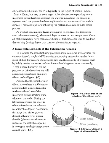
Assume that the small area of
silicon shown here is sufficient to
accommodate a single transistor
in the middle of one of the
integrated circuits residing some- middle of the silicon wafer
where on the wafer. During the
fabrication process the wafer is
often referred to as the substrate,
meaning “base layer.” A common
first stage is to either grow or
deposit a thin layer of silicon
dioxide (glass) across the entire
surface of the wafer by exposing
it to oxygen in a high-temperature
oven (Figure 14-4). Figure 14-4. Grow or deposit a
layer of silicon dioxide