
Page 163 - Bebop to The Boolean Boogie An Unconventional Guide to Electronics Fundamentals, Components, and Processes
P. 163
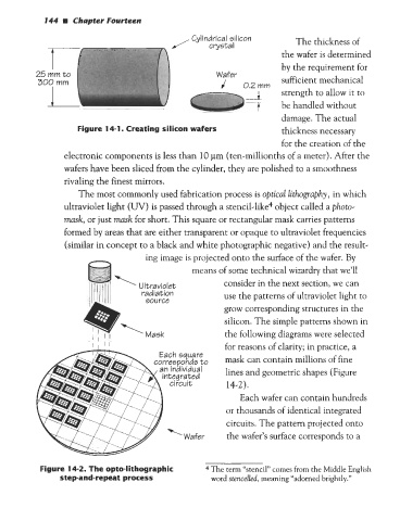
144  II Chapter Fourteen
                                                 Cylindrical silicon       The thickness of
                                            /  crysta~
                                                                        the wafer is determined
                                                                        by the requirement for
                                                       Wafer
                                                         J    0.2 mm    sufficient mechanical
                                                               A        strength to allow it to
                                                               t
                                                                        be handled without
                                                                        damage. The actual
                    Figure 14-1. Creating silicon wafers                thickness necessary
                                                                        for the creation of the
                 electronic components is less than 10 pm (ten-millionths of a meter). After the
                 wafers have been sliced from the cylinder, they are polished to a smoothness
                 rivaling the finest mirrors.
                     The most commonly used fabrication process is optical lithography, in which
                 ultraviolet light (UV) is passed through a stencil-like4 object called a photo-
                 mask, or just mask for short. This square or rectangular mask carries patterns
                 formed by areas that are either transparent or opaque to ultraviolet frequencies
                 (similar in concept to a black and white photographic negative) and the result-
                                      ing image is projected onto the surface of the wafer. By
                                                 means of some technical wizardry that we’ll
                                                         consider in the next section, we can
                                                         use the patterns of ultraviolet light to
                                      50urce
                                                         grow corresponding structures in the
                                                         silicon. The simple patterns shown in
                                                         the following diagrams were selected
                                                         for reasons of clarity; in practice, a
                                                          mask can contain millions of fine
                                                          lines and geometric shapes (Figure
                                                          14-2).
                                                             Each wafer can contain hundreds
                                                          or thousands of identical integrated
                                                          circuits. The pattern projected onto
                                                          the wafer’s surface corresponds to a


           Figure 14-2. The opto-lithographic        4 The term “stencil” comes from the Middle English
                stepand-repeat process                word stencelkd, meaning “adorned brightly.”