
Page 165 - Bebop to The Boolean Boogie An Unconventional Guide to Electronics Fundamentals, Components, and Processes
P. 165
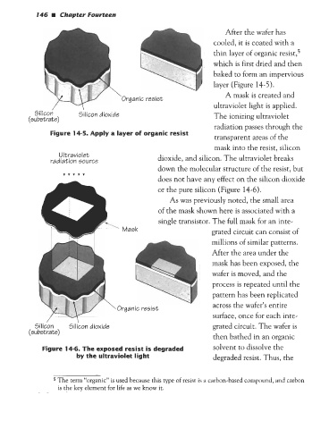
146  H  Chapter Fourteen

                                                                      After the wafer has
                                                                  cooled, it is coated with a
                                                                  thin layer of organic re~ist,~
                                                                  which is first dried and then
                                                                  baked to form an impervious
                                                                  layer (Figure 14-5).

                                      Organic resist                  A mask is created and
                                                                  ultraviolet light is applied.
            Silicon
          (su bstrate)   Silicon dioxide                          The ionizing ultraviolet
                                                                  radiation passes through the
                Figure 14-5. Apply a layer of organic resist
                                                                  transparent areas of the
                                                                  mask into the resist, silicon
                   Ultraviolet
                radiation source                 dioxide, and silicon. The ultraviolet breaks
                                                 down the molecular structure of  the resist, but

                                                 does not have any effect on the silicon dioxide
                                                 or the pure silicon (Figure 14-6).

                                                     As was previously noted, the small area
                                 I               of  the mask shown here is associated with a
                                                 single transistor. The full mask for an inte-
                                      Mask                        grated circuit can consist of

                                                                  millions of similar patterns.
                                                                  After the area under the
                                                                  mask has been exposed, the
                                                                  wafer is moved, and the
                                                                  process is repeated until the
                                                                  pattern has been replicated
                                     Organic resist               across the wafer’s entire
                                                                  surface, once for each inte-
           Sili&      Silicon dioxide                             grated circuit. The wafer is
          (su bstrate)
                                                                  then bathed in an organic
              Figure 14-6. The exposed resist is degraded         solvent to dissolve the
                        by the ultraviolet light                  degraded resist. Thus, the


                  The term “organic” is used because this type of resist is a carbon-based compound, and carbon
                  is the key element for life as we know it.