
Page 166 - Bebop to The Boolean Boogie An Unconventional Guide to Electronics Fundamentals, Components, and Processes
P. 166
Integrated Circuits (ICs) H I4 7
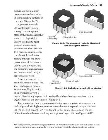
pattern on the mask has
been transferred to a series
of corresponding patterns in
the resist (Figure 14-7).
A process in which
ultraviolet light passing
through the transparent Organic resist
areas of the mask causes the
Silicon
resist to be degraded is (su bstxate) Silicon dioxide
known as a positive-resist Figure 14-7. The degraded resist is dissolved
process; negative-resist with an organic solvent
processes are also available.
In a negative-resist process,
the ultraviolet radiation
passing through the trans-
parent areas of the mask is
used to cure the resist, and
the remaining uncured areas
are then removed using an
appropriate solvent. Organic resist
After the unwanted
Silicon 5ilicon dioxide
resist has been removed, the (su bstrate)
wafer undergoes a process
Figure 14-8. Etch the exposed silicon dioxide
known as etching, in which
an appropriate solvent is
used to dissolve any exposed silicon dioxide without having any effect on the
organic resist or the pure silicon (Figure 14-8).
The remaining resist is then removed using an appropriate solvent, and the
wafer is placed in a high temperature oven where it is exposed to a gas contain-
ing the selected dopant (a P-type dopant in this case). The atoms in the gas
diffuse into the substrate resulting in a region of doped silicon (Figure 14-9).6
6 In some processes, diffusion is augmented with ion implantation techniques, in which beams of ions
are directed at the wafer to alter the type and conductivity of the silicon in selected regions.