
Page 167 - Bebop to The Boolean Boogie An Unconventional Guide to Electronics Fundamentals, Components, and Processes
P. 167
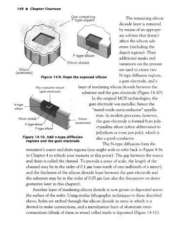
148 rn  Chapter Fourteen

                                         Gas containinq                 The remaining silicon

                                                                    dioxide layer is removed
                                                                    by means of an appropri-
                                                                    ate solvent that doesn’t
                                                                    affect the silicon sub-
                                                                    strate (including the
                                                                    doped regions). Then
                                                                    additional masks and
                                                                    variations on the process
                                                                    are used to create two
          (substrate)
                        Figure 14-9. Dope the exposed silicon       N-type diffusion regions,
                                                                    a gate electrode, and a
                     Poly-crystalline silicon   layer of insulating silicon dioxide between the
                       (gate electrode)        substrate and the gate electrode (Figure 14-10).
                   /         I
                                                     In the original MOS technologies, the
                                                   gate electrode was metallic: hence the
                                                     “metal-oxide semiconductor” appella-
                                                       tion. In modern processes, however,
                                           -  Silicon
                                            (substrate)   the gate electrode is formed from poly-
                                                       crystalline silicon (often abbreviated to
                                                       polysilicon or even just poly), which is
              Figure 14-1 0. Add n-type diffusion      also a good conductor.
                regions and the gate electrode
                                                           The N-type diffusions form the
                transistor’s source and drain regions (you might wish to refer back to Figure 4-9a
                in Chapter 4 to refresh your memory at this point). The gap between the source
                and drain is called the channel. To provide a sense of scale, the length of  the
                channel may be in the order of 0.1 pm (one-tenth of one-millionth of a meter),
                and the thickness of the silicon dioxide layer between the gate electrode and
                the substrate may be in the order of 0.05 pm (see also the discussions on dewice
                geometries later in this chapter).
                   Another layer of insulating silicon dioxide is now grown or deposited across
                the surface of the wafer. Using similar lithographic techniques to those described
                above, holes are etched through the silicon dioxide in areas in which it is
                desired to make connections, and a metalization layer of aluminum inter-
                connections (think of them as wires) called tracks is deposited (Figure 14-1 1).