
Page 172 - Bebop to The Boolean Boogie An Unconventional Guide to Electronics Fundamentals, Components, and Processes
P. 172
Integrated Circuits (ICs) 7 53
An individually packaged integrated circuit consists of the die and its
connections to the external leads, all encapsulated in the protective package,
The package protects the silicon from moisture and other impurities and helps
to conduct heat away from the die when the device is operating,
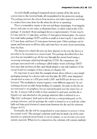
There is tremendous variety in the size and shape of packages. A rectangular
device with pins on two sides, as illustrated here, is called a dual in-line (DIL)
package. A standard 14-pin packaged device is approximately 18 mm long
6.5 mm wide by 2.5 mm deep, and has 2.5 mm spaces between pins. An equiva-
lent smll outline package (SOP) could be as small as 4 mm long by 2 mm wide by
0.75 mm deep, and have 0.5 rnm spaces between pins. Other packages can be
square and have pins on all four sides, and some have an array of pins protruding
from the base.
The shapes into which the pins are bent depend on the way the device is
intended to be mounted on a circuit board. The package described above has
pins that are intended to go all the way through the circuit board using a
mounting technique called lead through hole (LTH). By comparison, the
packages associated with a technique called surface mount technology (SMT)
have pins that are bent out flat, and which attach to one side (surface) of the
circuit board (an example of this is shown in Chapter 18).
It’s important to note that the example shown above reflects a very simple
packaging strategy for a device with very few pins. By 2002, some integrated
circuits had as many as 1,000 pins (with 2,000- and 4,000-pin devices on the
horizon). This multiplicity of pins requires a very different approach. In one
technique known as solder bump bonding, for example, the pads on the die are
not restricted to its periphery, but are instead located over the entire face of
the die. A minute ball of solder is then attached to each pad, and the die is
flipped over and attached to the package substrate (this is referred to as a
“flip-chip” technique). Each pad on the die has a corresponding pad on the
package substrate, and the package-die combo is heated so as to melt the solder
balls and form good electrical connections between the die and the substrate
(Figure 14-17).
Eventually, the die will be encapsulated in some manner to protect it from
the outside world. The package’s substrate itself may be made out of the same
material as a printed circuit board, or out of ceramic, or out of some even more
esoteric material. Whatever its composition, the substrate will contain multiple