
Page 289 - Build Your Own Transistor Radios a Hobbyists Guide to High-Performance and Low-Powered Radio Circuits
P. 289
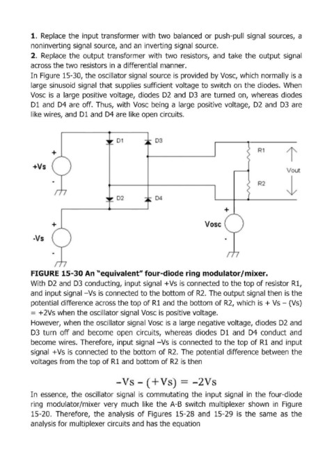
1.  Replace  the  input transformer with  two  balanced  ог push-pull  signal  sources,  а

            noninveгting signal source, and  ап inveгting signal  source.
            2.  Replace  the  output transformer  with  two  resistors,  and  take  the  output  sigпаl
            across the two resistors in  а differential  mаппег.
            In Figure 15-30, the oscillator signal source is provided  Ьу Vosc,  which  normally is  а
            large sinusoid  signal  that supplies sufficient voltage to switch  оп the diodes.  When

            Vosc  is  а large  positive  voltage,  diodes  О2 and  DЗ аге turned  оп, whereas  diodes
            О1 and  О4 аге off.  Thus,  with  Vosc  being  а large  positive  voltage,  О2 and  DЗ аге
            like wires, and  О1 and  О4 аге like ореп circuits.


                                           01            DЗ
                                                                                             R1

             +V
                                                                                                        Vo
                                                                                               2


                    +                                                     Vosc

             .. V


            FIGURE 15-30 Ап "equivalent" four-diode ring modulator/mixer.

            With  О2 and  О3 conducting,input signal  +Vs is connected to the top of resistor R1,
            an,d input sigпаl -Vs is connected to the bottom of R2.  The output signal then is the
            potentialdifference across the top of R1  and the bottom of R2,  which  is + Vs - (Vs)
            = +2Vs when the oscillator sigпаl Vosc  is positive voltage.

            However, when the oscillator signal Voscis а large negative voltage, diodes О2 and
            DЗ turn  off and  Ьесоте ореп circuits,  whereas  diodes  О1 and  О4 conduct  апd
            Ьесоте wires.  Therefore,  input signal  -Vs is  connected  to the top of R1  and  input
            signal  +Vs is  connected  to the bottom of R2.  The  potential  diffегепсе between  the
            voltages from the top of R1  and bottom of R2  is thеп


            Iп  еssепсе, the  oscillator signal  is  соmmutаtiiпg the  iпрut signal  in  the  four-diode
            ring  modulator/mixer  уегу much  like  the  Д-В switch  multiplexer  shown  in  Figure
            15-20.  Therefore,  the  апаlуsis of  Figures  15-28  and  15-29  is  the  samle  as  the
            analysis for multiplexer circuits and  has the equation