
Page 95 - Build Your Own Transistor Radios a Hobbyists Guide to High-Performance and Low-Powered Radio Circuits
P. 95
L ow e vel
L
,,1/ 1 Audio
RF Antenna Filter RF/AF Amplifier Det
-
L 1-VC1 Q1 03
I
+ 1.5 to 3 Audio Out
C2
~Uf L2
R1 3.9 mH or 4.7 mH R5
C7
100K
.01 ut
• L 1 Primary
VC1 RF VC10sc
470 uh 1 IN 34 or Germanium
140 pf
60 pt T1
C3
.0022 ut
.01 ut C6
• L 1 Secondary 1 uf
_uh
2
C4 R2
C5
1K
1 11N914 1K
100 ut R4
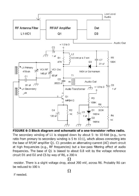
FIGURE 6-3 Block diagram and schematic of a one-transistor reflex radio.
The secondary winding of L1 is stepped down by about 5- to 10-fold (e.g., turns
ratio from primary to secondary winding is 5 to 10: 1), which allows connecting into
the base of RF/ AF amplifier Ql. Cl provides an alternating-current (AC) short circuit
at high frequencies (e.g., RF frequencies) but a low-pass filtering effect at audio
frequencies. The base of Q1 is biased to about 0.8 volt by the voltage reference
circuit D1 and D2 and CS by way of R6, a 200-k
resistor. There is a slight voltage drop, about 200 mV, across R6. Probably R6 can
be reduced to 100 k
if needed.