
Page 246 - Complete Wireless Design
P. 246
Oscillator Design
Oscillator Design 245
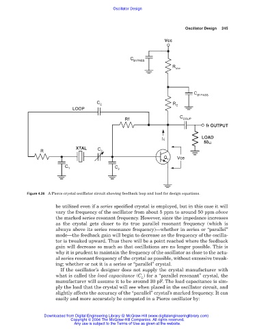
Figure 4.26 A Pierce crystal oscillator circuit showing feedback loop and load for design equations.
be utilized even if a series specified crystal is employed, but in this case it will
vary the frequency of the oscillator from about 5 ppm to around 50 ppm above
the marked series resonant frequency. However, since the impedance increases
as the crystal gets closer to its true parallel resonant frequency (which is
always above its series resonance frequency)—whether in series or “parallel”
mode—the feedback gain will begin to decrease as the frequency of the oscilla-
tor is tweaked upward. Thus there will be a point reached where the feedback
gain will decrease so much so that oscillations are no longer possible. This is
why it is prudent to maintain the frequency of the oscillator as close to the actu-
al series resonant frequency of the crystal as possible, without excessive tweak-
ing; whether or not it is a series or “parallel” crystal.
If the oscillator’s designer does not supply the crystal manufacturer with
what is called the load capacitance (C ) for a “parallel resonant” crystal, the
L
manufacturer will assume it to be around 30 pF. The load capacitance is sim-
ply the load that the crystal will see when placed in the oscillator circuit, and
slightly affects the accuracy of the “parallel” crystal’s marked frequency. It can
easily and more accurately be computed in a Pierce oscillator by:
Downloaded from Digital Engineering Library @ McGraw-Hill (www.digitalengineeringlibrary.com)
Copyright © 2004 The McGraw-Hill Companies. All rights reserved.
Any use is subject to the Terms of Use as given at the website.