
Page 247 - Complete Wireless Design
P. 247
Oscillator Design
246 Chapter Four
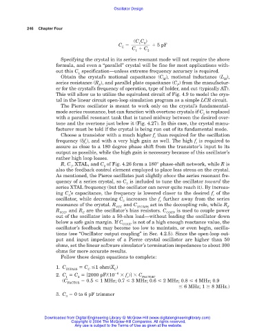
(C C )
1
2
C 5 pF
L
C C
1 2
Specifying the crystal in its series resonant mode will not require the above
formula, and even a “parallel” crystal will be fine for most applications with-
out this C specification—unless extreme frequency accuracy is required.
L
Obtain the crystal’s motional capacitance (C ), motional inductance (L ),
M M
series resistance (R ), and parallel plate capacitance (C ) from the manufactur-
S P
er for the crystal’s frequency of operation, type of holder, and cut (typically AT).
This will allow us to utilize the equivalent circuit of Fig. 4.9 to model the crys-
tal in the linear circuit open-loop simulation program as a simple LCR circuit.
The Pierce oscillator is meant to work only on the crystal’s fundamental-
mode series resonance, but can function with overtone crystals if C is replaced
1
with a parallel resonant tank that is tuned midway between the desired over-
tone and the overtone just below it (Fig. 4.27). In this case, the crystal manu-
facturer must be told if the crystal is being run out of its fundamental mode.
Choose a transistor with a much higher f than required for the oscillation
t
frequency (5f ), and with a very high gain as well. The high f is required to
t t
assure as close to a 180 degree phase shift from the transistor’s input to its
output as possible, while the high gain is necessary because of this oscillator’s
rather high loop losses.
R, C , XTAL, and C of Fig. 4.26 form a 180° phase-shift network, while R is
1 2
also the feedback control element employed to place less stress on the crystal.
As mentioned, the Pierce oscillates just slightly above the series resonant fre-
quency of a series crystal, so C is included to tune the oscillator toward the
3
series XTAL frequency (but the oscillator can never quite reach it). By increas-
ing C ’s capacitance, the frequency is lowered closer to the desired f of the
3 r
oscillator, while decreasing C increases the f further away from the series
3 r
resonance of the crystal. R and C act in the decoupling role, while R ,
VCC BYPASS f
R , and R are the oscillator’s bias resistors. C is used to couple power
VCC C COUP
out of the oscillator into a 50-ohm load—without loading the oscillator down
below a safe gain margin. If C is not of a high enough reactance value, the
COUP
oscillator’s feedback may become too low to maintain, or even begin, oscilla-
tions (see “Oscillator output coupling” in Sec. 4.2.5). Since the open-loop out-
put and input impedance of a Pierce crystal oscillator are higher than 50
ohms, set the linear software simulator’s termination impedances to about 300
ohms for more accurate results.
Follow these design equations to complete:
1. C C 1 ohm(X )
BYPASS C C
2. C C [2000 pF/(10 6
f )]
C .
1 2 r FACTOR
(C 0.5 1 MHz; 0.7 3 MHz; 0.6 2 MHz; 0.8 4 MHz; 0.9
FACTOR
6 MHz; 1 8 MHz.)
3. C 0 to 6 pF trimmer
3
Downloaded from Digital Engineering Library @ McGraw-Hill (www.digitalengineeringlibrary.com)
Copyright © 2004 The McGraw-Hill Companies. All rights reserved.
Any use is subject to the Terms of Use as given at the website.