
Page 428 - Complete Wireless Design
P. 428
Wireless Issues
Wireless Issues 427
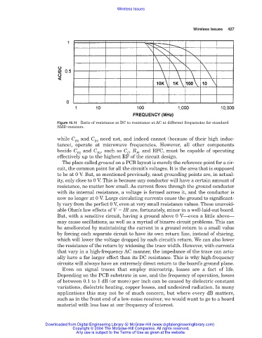
Figure 10.11 Ratio of resistance at DC to resistance at AC at different frequencies for standard
SMD resistors.
while C and C need not, and indeed cannot (because of their high induc-
B2 B3
tance), operate at microwave frequencies. However, all other components
beside C and C , such as C , R , and RFC, must be capable of operating
B2 B3 C B
effectively up to the highest RF of the circuit design.
The place called ground on a PCB layout is merely the reference point for a cir-
cuit, the common point for all the circuit’s voltages. It is the area that is supposed
to be at 0 V. But, as mentioned previously, most grounding points are, in actual-
ity, only close to 0 V. This is because any conductor will have a certain amount of
resistance, no matter how small. As current flows through the ground conductor
with its internal resistance, a voltage is formed across it, and the conductor is
now no longer at 0 V. Large circulating currents cause the ground to significant-
ly vary from the perfect 0 V, even at very small resistance values. These unavoid-
able Ohm’s law effects of V IR are, fortunately, minor in a well-laid-out board.
But, with a sensitive circuit, having a ground above 0 V—even a little above—
may cause oscillations, as well as a myriad of bizarre circuit problems. This can
be ameliorated by maintaining the current in a ground return to a small value
by forcing each separate circuit to have its own return line, instead of sharing,
which will lower the voltage dropped by each circuit’s return. We can also lower
the resistance of the return by widening the trace width. However, with currents
that vary in a high-frequency AC manner, the impedance of the trace can actu-
ally have a far larger effect than its DC resistance. This is why high-frequency
circuits will always have an extremely direct return to the board’s ground plane.
Even on signal traces that employ microstrip, losses are a fact of life.
Depending on the PCB substrate in use, and the frequency of operation, losses
of between 0.1 to 1 dB (or more) per inch can be caused by dielectric constant
variations, dielectric heating, copper losses, and undesired radiation. In many
applications this may not be of much concern, but where every dB matters,
such as in the front end of a low-noise receiver, we would want to go to a board
material with less loss at our frequency of interest.
Downloaded from Digital Engineering Library @ McGraw-Hill (www.digitalengineeringlibrary.com)
Copyright © 2004 The McGraw-Hill Companies. All rights reserved.
Any use is subject to the Terms of Use as given at the website.