
Page 425 - Complete Wireless Design
P. 425
Wireless Issues
424 Chapter Ten
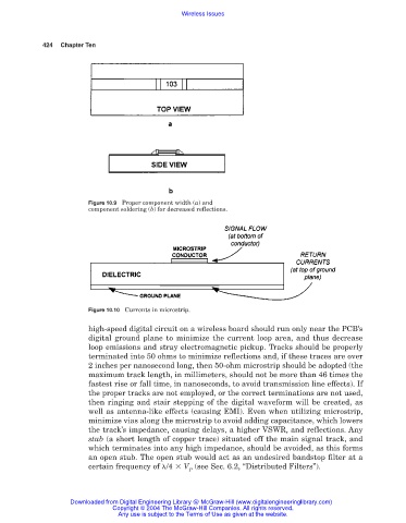
Figure 10.9 Proper component width (a) and
component soldering (b) for decreased reflections.
Figure 10.10 Currents in microstrip.
high-speed digital circuit on a wireless board should run only near the PCB’s
digital ground plane to minimize the current loop area, and thus decrease
loop emissions and stray electromagnetic pickup. Tracks should be properly
terminated into 50 ohms to minimize reflections and, if these traces are over
2 inches per nanosecond long, then 50-ohm microstrip should be adopted (the
maximum track length, in millimeters, should not be more than 46 times the
fastest rise or fall time, in nanoseconds, to avoid transmission line effects). If
the proper tracks are not employed, or the correct terminations are not used,
then ringing and stair stepping of the digital waveform will be created, as
well as antenna-like effects (causing EMI). Even when utilizing microstrip,
minimize vias along the microstrip to avoid adding capacitance, which lowers
the track’s impedance, causing delays, a higher VSWR, and reflections. Any
stub (a short length of copper trace) situated off the main signal track, and
which terminates into any high impedance, should be avoided, as this forms
an open stub. The open stub would act as an undesired bandstop filter at a
certain frequency of /4 V (see Sec. 6.2, “Distributed Filters”).
P
Downloaded from Digital Engineering Library @ McGraw-Hill (www.digitalengineeringlibrary.com)
Copyright © 2004 The McGraw-Hill Companies. All rights reserved.
Any use is subject to the Terms of Use as given at the website.