
Page 421 - Complete Wireless Design
P. 421
Wireless Issues
420 Chapter Ten
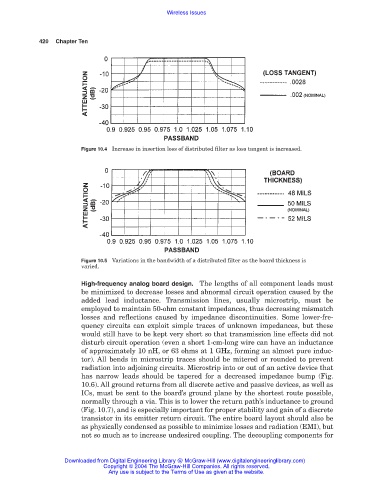
Figure 10.4 Increase in insertion loss of distributed filter as loss tangent is increased.
Figure 10.5 Variations in the bandwidth of a distributed filter as the board thickness is
varied.
High-frequency analog board design. The lengths of all component leads must
be minimized to decrease losses and abnormal circuit operation caused by the
added lead inductance. Transmission lines, usually microstrip, must be
employed to maintain 50-ohm constant impedances, thus decreasing mismatch
losses and reflections caused by impedance discontinuities. Some lower-fre-
quency circuits can exploit simple traces of unknown impedances, but these
would still have to be kept very short so that transmission line effects did not
disturb circuit operation (even a short 1-cm-long wire can have an inductance
of approximately 10 nH, or 63 ohms at 1 GHz, forming an almost pure induc-
tor). All bends in microstrip traces should be mitered or rounded to prevent
radiation into adjoining circuits. Microstrip into or out of an active device that
has narrow leads should be tapered for a decreased impedance bump (Fig.
10.6). All ground returns from all discrete active and passive devices, as well as
ICs, must be sent to the board’s ground plane by the shortest route possible,
normally through a via. This is to lower the return path’s inductance to ground
(Fig. 10.7), and is especially important for proper stability and gain of a discrete
transistor in its emitter return circuit. The entire board layout should also be
as physically condensed as possible to minimize losses and radiation (EMI), but
not so much as to increase undesired coupling. The decoupling components for
Downloaded from Digital Engineering Library @ McGraw-Hill (www.digitalengineeringlibrary.com)
Copyright © 2004 The McGraw-Hill Companies. All rights reserved.
Any use is subject to the Terms of Use as given at the website.