
Page 422 - Complete Wireless Design
P. 422
Wireless Issues
Wireless Issues 421
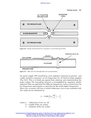
Figure 10.6 Proper board layout for a transistor as seen from top of PCB.
Figure 10.7 Side view of a through-hole via to ground plane.
the power supply (PS) should have a low capacitive reactance to ground—and
a high inductive reactance—at all frequencies for all devices being supplied
(Fig. 10.8). This is to block any signals from entering, and contaminating, the
power supply. The decoupling function is accomplished by capacitors (and/or
inductors) that are optimized for different frequencies; such as electrolytics for
low frequencies and ceramics or porcelain for the much higher frequencies.
Since vias, as stated, will have a certain inductance, just as any conductor will,
this value can be calculated by:
4h
L 5.08h ln 1
d
where L inductance of the via, nH
h length of the via, inches
d diameter of the via, inches
Downloaded from Digital Engineering Library @ McGraw-Hill (www.digitalengineeringlibrary.com)
Copyright © 2004 The McGraw-Hill Companies. All rights reserved.
Any use is subject to the Terms of Use as given at the website.