
Page 456 - Complete Wireless Design
P. 456
Wireless Issues
Wireless Issues 455
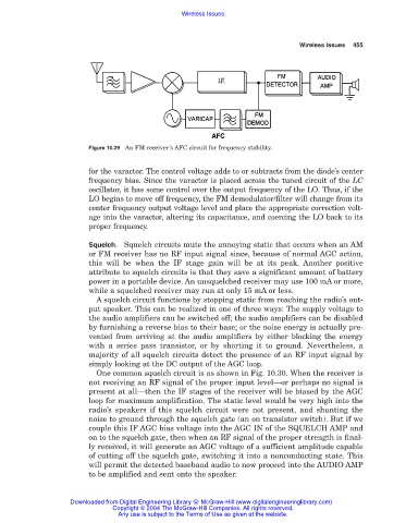
Figure 10.29 An FM receiver’s AFC circuit for frequency stability.
for the varactor. The control voltage adds to or subtracts from the diode’s center
frequency bias. Since the varactor is placed across the tuned circuit of the LC
oscillator, it has some control over the output frequency of the LO. Thus, if the
LO begins to move off frequency, the FM demodulator/filter will change from its
center frequency output voltage level and place the appropriate correction volt-
age into the varactor, altering its capacitance, and coercing the LO back to its
proper frequency.
Squelch. Squelch circuits mute the annoying static that occurs when an AM
or FM receiver has no RF input signal since, because of normal AGC action,
this will be when the IF stage gain will be at its peak. Another positive
attribute to squelch circuits is that they save a significant amount of battery
power in a portable device. An unsquelched receiver may use 100 mA or more,
while a squelched receiver may run at only 15 mA or less.
A squelch circuit functions by stopping static from reaching the radio’s out-
put speaker. This can be realized in one of three ways: The supply voltage to
the audio amplifiers can be switched off; the audio amplifiers can be disabled
by furnishing a reverse bias to their base; or the noise energy is actually pre-
vented from arriving at the audio amplifiers by either blocking the energy
with a series pass transistor, or by shorting it to ground. Nevertheless, a
majority of all squelch circuits detect the presence of an RF input signal by
simply looking at the DC output of the AGC loop.
One common squelch circuit is as shown in Fig. 10.30. When the receiver is
not receiving an RF signal of the proper input level—or perhaps no signal is
present at all—then the IF stages of the receiver will be biased by the AGC
loop for maximum amplification. The static level would be very high into the
radio’s speakers if this squelch circuit were not present, and shunting the
noise to ground through the squelch gate (an on transistor switch). But if we
couple this IF AGC bias voltage into the AGC IN of the SQUELCH AMP and
on to the squelch gate, then when an RF signal of the proper strength is final-
ly received, it will generate an AGC voltage of a sufficient amplitude capable
of cutting off the squelch gate, switching it into a nonconducting state. This
will permit the detected baseband audio to now proceed into the AUDIO AMP
to be amplified and sent onto the speaker.
Downloaded from Digital Engineering Library @ McGraw-Hill (www.digitalengineeringlibrary.com)
Copyright © 2004 The McGraw-Hill Companies. All rights reserved.
Any use is subject to the Terms of Use as given at the website.