
Page 150 - Electrical Properties of Materials
P. 150
132 Semiconductors
E
F
which leads to a quadratic equation in x, giving finally for the Fermi level,
E E F = 0.97 eV. Thus, in the practical case of an extrinsic semiconductor the
g
E Fermi level is considerably above the middle of the energy gap.
D
Let us consider now the variation of Fermi level with temperature. This is
1 2 3
somewhat complicated by the fact that E g and E D are dependent on lattice
E dimensions, and hence both change with temperature, but we shall ignore this
g E
2 Fi effect for the moment.
At very low temperatures (a few degrees absolute), the chance of excitation
across the gap is fantastically remote compared with the probability of ioniza-
0 tion from a donor level (which is only remote). Try calculating this for a 1 eV
0 T 28
value of E g and a 0.05 eV value of E g – E D . You should find that with 10
lattice atoms per cubic metre, of which only 10 21 are donors, practically all the
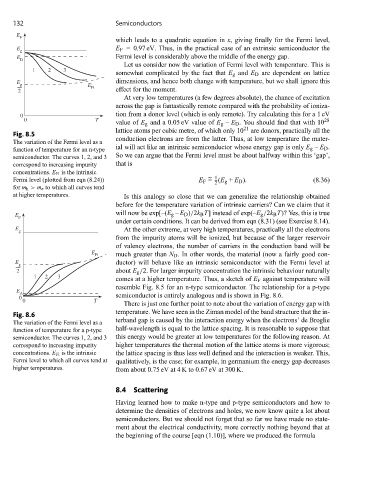
Fig. 8.5
The variation of the Fermi level as a conduction electrons are from the latter. Thus, at low temperature the mater-
function of temperature for an n-type ial will act like an intrinsic semiconductor whose energy gap is only E g – E D .
semiconductor. The curves 1, 2, and 3 So we can argue that the Fermi level must be about halfway within this ‘gap’,
correspond to increasing impurity that is
concentrations. E Fi is the intrinsic
~ 1
Fermi level (plotted from eqn (8.24)) E F = (E g + E D ). (8.36)
2
for m h > m e to which all curves tend
at higher temperatures. Is this analogy so close that we can generalize the relationship obtained
before for the temperature variation of intrinsic carriers? Can we claim that it
will now be exp[–(E g – E D )/2k B T] instead of exp(–E g /2k B T)? Yes, this is true
E
F
under certain conditions. It can be derived from eqn (8.31) (see Exercise 8.14).
E At the other extreme, at very high temperatures, practically all the electrons
g
from the impurity atoms will be ionized, but because of the larger reservoir
of valency electrons, the number of carriers in the conduction band will be
E Fi much greater than N D . In other words, the material (now a fairly good con-
E ductor) will behave like an intrinsic semiconductor with the Fermi level at
g
2 about E g /2. For larger impurity concentration the intrinsic behaviour naturally
1 2 3
comes at a higher temperature. Thus, a sketch of E F against temperature will
resemble Fig. 8.5 for an n-type semiconductor. The relationship for a p-type
E
A
0 semiconductor is entirely analogous and is shown in Fig. 8.6.
0 T
There is just one further point to note about the variation of energy gap with
temperature. We have seen in the Ziman model of the band structure that the in-
Fig. 8.6
The variation of the Fermi level as a terband gap is caused by the interaction energy when the electrons’ de Broglie
function of temperature for a p-type half-wavelength is equal to the lattice spacing. It is reasonable to suppose that
semiconductor. The curves 1, 2, and 3 this energy would be greater at low temperatures for the following reason. At
correspond to increasing impurity higher temperatures the thermal motion of the lattice atoms is more vigorous;
concentrations. E Fi is the intrinsic the lattice spacing is thus less well defined and the interaction is weaker. This,
Fermi level to which all curves tend at qualitatively, is the case; for example, in germanium the energy gap decreases
higher temperatures. from about 0.75 eV at 4 K to 0.67 eV at 300 K.
8.4 Scattering
Having learned how to make n-type and p-type semiconductors and how to
determine the densities of electrons and holes, we now know quite a lot about
semiconductors. But we should not forget that so far we have made no state-
ment about the electrical conductivity, more correctly nothing beyond that at
the beginning of the course [eqn (1.10)], where we produced the formula