
Page 306 - Electrical Properties of Materials
P. 306
288 Magnetic materials
of spin-up electrons declines and the number of spin-down electrons increases
then it is not unreasonable to talk about a spin current. Theoretical physicists
(a) have quite a complicated definition: they say the spin current is a tensor. We
don’t need to go into any of the complications. We shall just use the simplified
definition,
J = J up – J down . (11.51)
The variation of the magnetization in the two materials is shown in
F 1 N F 2 Fig. 11.24(b). There is a tendency towards spin equilibrium in N, hence the
spin current must decline. How fast will it decline? We may introduce a ‘dif-
fusion length’ or ‘coherence length’ to describe the distance, after which the
(b)
number of electrons with spin up declines by a factor of e. Practical values for
a non-magnetic metal are between 100 nm and 1 μm. Note that the coherence
length is much longer in semiconductors than in metals. It extends from a few
μm to about 100 μm.
Have we seen similar phenomena before? The situation is analogous to an
N
F 1 F 2 n–i junction, i.e. a junction between an n-type and an intrinsic semiconductor.
When a forward voltage is applied the electrons are injected into the intrinsic
material. There will be an excess of electrons over holes there but eventually
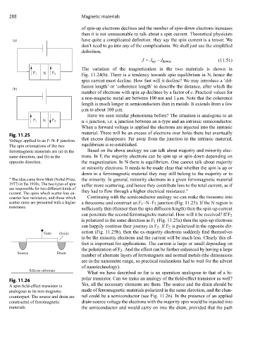
Fig. 11.25
Voltage applied to an F–N–F junction. that excess disappears. Far away from the junction in the intrinsic material,
The spin orientations of the two equilibrium is re-established.
ferromagnetic materials are (a) in the Based on the above analogy we can talk about majority and minority elec-
same direction, and (b) in the trons. In F, the majority electrons can be spin up or spin down depending on
opposite direction. the magnetization. In N there is equilibrium. One cannot talk about majority
or minority electrons. It needs to be made clear that whether the spin is up or
down in a ferromagnetic material they may still belong to the majority or to
∗ The idea came from Mott (Nobel Prize, the minority. In general, minority electrons in a given ferromagnetic material
1977) in the 1930s. The two types of spin suffer more scattering, and hence they contribute less to the total current, as if
are responsible for two different kinds of ∗
current. The spins which scatter less en- they had to flow through a higher electrical resistance.
counter less resistance, and those which Continuing with the semiconductor analogy we can make the twosome into
scatter more are presented with a higher a threesome and construct an F 1 –N–F 2 junction (Fig. 11.25). If the N region is
resistance.
sufficiently thin (thinner than the spin diffusion length) then the spin-up current
can penetrate the second ferromagnetic material. How will it be received? If F 2
is polarized in the same direction as F 1 (Fig. 11.25a) then the spin-up electrons
can happily continue their journey in F 2 .IfF 2 is polarized in the opposite dir-
ection (Fig. 11.25b), then the ex-majority electrons suddenly find themselves
Gate Oxide
to be the minority electrons and the current will be much less. Clearly this ef-
fect is important for applications. The current is large or small depending on
the polarization of F 2 . And the effect can be further enhanced by having a large
Source Drain
number of alternate layers of ferromagnets and normal metals (the dimensions
are in the nanometre range, so practical realizations had to wait for the advent
of nanotechnology).
Silicon substrate
What we have described so far is an operation analogous to that of a bi-
polar transistor. Can we make an analogy of the field-effect transistor as well?
Fig. 11.26
Yes, all the necessary elements are there. The source and the drain should be
A spin field-effect transistor is
analogous to its non-magnetic made of ferromagnetic materials polarized in the same direction, and the chan-
counterpart. The source and drain are nel could be a semiconductor (see Fig. 11.26). In the presence of an applied
constructed of ferromagnetic drain-source voltage the electrons with the majority spin would be injected into
materials. the semiconductor and would carry on into the drain, provided that the path