Page 121 - Environmental Nanotechnology Applications and Impacts of Nanomaterials
P. 121
Methods for Structural and Chemical Characterization of Nanomaterials  107

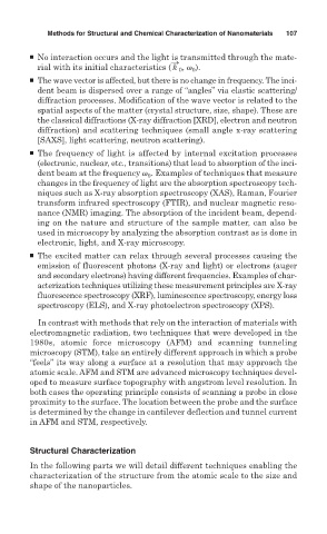
        ■ No interaction occurs and the light is transmitted through the mate-
                                           S
          rial with its initial characteristics ( k 0 , v 0 ).
        ■ The wave vector is affected, but there is no change in frequency. The inci-
          dent beam is dispersed over a range of “angles” via elastic scattering/
          diffraction processes. Modification of the wave vector is related to the
          spatial aspects of the matter (crystal structure, size, shape). These are
          the classical diffractions (X-ray diffraction [XRD], electron and neutron
          diffraction) and scattering techniques (small angle x-ray scattering
          [SAXS], light scattering, neutron scattering).
        ■ The frequency of light is affected by internal excitation processes
          (electronic, nuclear, etc., transitions) that lead to absorption of the inci-
                                      . Examples of techniques that measure
          dent beam at the frequency v 0
          changes in the frequency of light are the absorption spectroscopy tech-
          niques such as X-ray absorption spectroscopy (XAS), Raman, Fourier
          transform infrared spectroscopy (FTIR), and nuclear magnetic reso-
          nance (NMR) imaging. The absorption of the incident beam, depend-
          ing on the nature and structure of the sample matter, can also be
          used in microscopy by analyzing the absorption contrast as is done in
          electronic, light, and X-ray microscopy.
        ■ The excited matter can relax through several processes causing the
          emission of fluorescent photons (X-ray and light) or electrons (auger
          and secondary electrons) having different frequencies. Examples of char-
          acterization techniques utilizing these measurement principles are X-ray
          fluorescence spectroscopy (XRF), luminescence spectroscopy, energy loss
          spectroscopy (ELS), and X-ray photoelectron spectroscopy (XPS).
          In contrast with methods that rely on the interaction of materials with
        electromagnetic radiation, two techniques that were developed in the
        1980s, atomic force microscopy (AFM) and scanning tunneling
        microscopy (STM), take an entirely different approach in which a probe
        “feels” its way along a surface at a resolution that may approach the
        atomic scale. AFM and STM are advanced microscopy techniques devel-
        oped to measure surface topography with angstrom level resolution. In
        both cases the operating principle consists of scanning a probe in close
        proximity to the surface. The location between the probe and the surface
        is determined by the change in cantilever deflection and tunnel current
        in AFM and STM, respectively.


        Structural Characterization
        In the following parts we will detail different techniques enabling the
        characterization of the structure from the atomic scale to the size and
        shape of the nanoparticles.

