
Page 391 - Fiber Fracture
P. 391
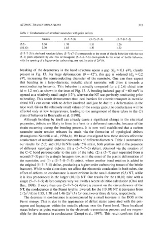
ATOMIC TRANSFORMATIONS                                              373

             Table 1. Conductances of armchair nanotubes with point defects

                         Pristine     (5-7-7-3       (5-7)-(7-5)     (5-7-8-7-3
             (53         2.00          I .70         1.11            I .26
             (10,IO)     2.00         1.85           I .33           I .72
             (5-7-7-5)  is the bond rotation defect; (5-7H7-5)  corresponds to the onset of plastic behavior with the two
             (5-7)  pairs  separated by  one row  of  hexagons; (5-74-7-5)   corresponds to  the onset of brittle behavior.
             with the opening of a higher-order carbon ring, see text. In  units of 2e2/h.


             breaking of  the degeneracy in the band  structure opens a gap (Eg x 0.1  eV), clearly
             present in  Fig.  13. For large deformations (0 = 42"),  this gap is widened (E, = 0.2
             eV), increasing the  semiconducting character of  the  nanotube. One can  then  expect
             that  bending  in  a  large-diameter, metallic  chiral  nanotube  will  drive  it  towards  a
             semiconducting behavior. This behavior is actually computed for a (1  2,6) chiral tube
             (d = 1.2 nm), as shown in the inset of Fig. 13. A bending-induced gap of -60  meV is
             opened at a relatively small angle (12"),  whereas the NT was perfectly conducting prior
             to bending. This result demonstrates that local barriers for electric transport in metallic
             chiral NTs can occur with no defect involved and just be due to a deformation in the
             tube wall. Given the relatively small values of the energy gaps, the conductance will be
             affected only at low temperatures, leading to the assignment of these tubes to the (3)
             class of behavior in Bezryadin et al. (1 998).
               Although bending by  itself can already cause a significant change in the electrical
             properties, defects are likely to form in a bent or a deformed nanotube, because of the
             strain occurring during the bending process. It is now  well established that a carbon
             nanotube  under  tension  releases  its  strain  via  the  formation  of  topological  defects
             (Buongiorno Nardelli et al., 1998a,b). We have investigated how these defects affect the
             conductance of metallic armchair nanotubes of different diameters. Table 1 summarizes
             our results for (53) and (1 0,lO) NTs under 5% strain, both pristine and in the presence
             of  different topological defects: (1) a  (5-7-7-5)   defect, obtained via the rotation of
             the C-C  bond perpendicular to the axis of the tube; (2) a (5-7)  pair separated from a
             second (7-5)  pair by a single hexagon row, as in the onset of the plastic deformation of
             the nanotube; and (3) a (5-7-8-7-5)   defect, where another bond rotation is added to
             the original (5-7-7-5)  defect, producing a higher-order carbon ring (onset of the brittle
             fracture). While strain alone does not affect the electronic conduction in both tubes, the
             effect of defects on conductance is more evident in the small-diameter (53) NT, while
             it is less pronounced in the larger (10,lO) NT. Our results for the (10,lO) tube with a
             single (5-7-7-5)  defect compare very well with a recent ab initio calculation (Choi and
             Ihm,  1999). If  more than one (5-7-7-5)   defect is present on the circumference of  the
             NT, the conductance at the Fermi level is lowered: for the (10,lO) NT it decreases from
             2 (2e2/ h) to I .95, I .70 and 1.46 (2e2/ h) for one, two or three defects, respectively.
               The decrease in conductance is accompanied by  a small increase in the DOS at the
             Fermi energy. This is due to the appearance of  defect states associated with the pen-
             tagons and heptagons within the metallic plateau near the Fermi level. These localized
             states behave as point scatterers in the electronic transmission process and are respon-
             sible for the decrease in conductance (Crespi et al.,  1997). This result confirms that in