
Page 284 - Fundamentals of Light Microscopy and Electronic Imaging
P. 284
CCD ARCHITECTURES 267
benefit being about a 10-fold reduction in the number of thermoelectrons for every 20°C
decrease in temperature. Thermal noise can be reduced significantly by cooling the CCD
down to 20°C or lower using a stack of 2–3 Peltier thermoelectric cooling devices. In
the presence of a current, a Peltier bimetallic strip becomes cold on one side and hot on
the other. The cold surface is mounted so that it is in indirect physical contact with the
CCD, while the heat on the other surface is removed by a fan or backed by a circulating
liquid cooling system. Astronomical cameras used for hour-long exposures are cooled
with liquid nitrogen. For biological specimens, acceptable images can be obtained from
exposures lasting just a few seconds or less from CCD cameras cooled to 0–10°C, but for
higher-quality, lower-noise images, deeper cooling to 25°C to 40°C is required. We
will deal with the noise components in a CCD image later in the chapter.
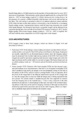
CCD ARCHITECTURES
CCD imagers come in three basic designs, which are shown in Figure 14-8 and
described as follows:
• Full-frame CCD. In this design, whose readout procedure was described in the pre-
ceding section, every pixel of the CCD surface contributes to the image. Exposures
are usually controlled by an electromechanical shutter, since the imaging surface
must be protected from incident light during readout of the CCD. Full-frame CCD
imagers are used for specimens requiring high dynamic range images and where the
time resolution can be on the order of a second or longer. The fastest frame rates in
so-called subarray mode are 10 frames/s and are limited by an electromechanical
shutter.
• Frame-transfer CCD. Cameras with frame-transfer CCDs are fast because expo-
sure and readout occur simultaneously. One-half of an elongated rectangular CCD
chip is masked at one end by an opaque cover (an aluminum coating on one-half of
the surface of the CCD), which is used as a storage buffer. After an exposure, all of
the pixels in the image half of the chip are transferred to pixels on the storage side
in 1 ms; the storage array is read out while the image array is being exposed for the
next picture. No camera shutter is needed because the time required for transfer
from the imaging area to the masked area ( 1 ms) is only a fraction of the time
needed for an exposure. A disadvantage is that only one-half of the potential imag-
ing surface of the chip can be used for imaging. Cameras of this type are chosen for
monitoring rapid kinetic processes such as in dye ratio imaging, where it is impor-
tant to maintain high spatial resolution and dynamic range.
Full frame Frame transfer Interline transfer
Storage
Image Storage
Image
Figure 14-8
Types of CCD designs. (a) Full-frame CCD. (b) Frame-transfer CCD. (c) Interline-transfer
CCD.